
Service manual

11
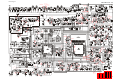
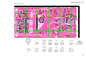
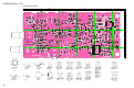
Circuit Description
Receive Signal Path
Incoming RF from the antenna jack is delivered to the
RF Unit and passes through a low-pass filter consisting of
coils L1001, L1002, and L1031, capacitors C1004, C1005,
C1008, C1010, C1014, C1016, and C1221, and antenna
switching diode D1003 (RLS135 TE-17).
Signals within the frequency range of the transceiver
enter a varactor-tuned band-pass filter consisting of coils
L1010 and L1011, capacitors C1044, C1046, C1060,
C1065, and C1068, and diodes D1011, D1012, D1013,
and D1014 (all HVC358B), then are amplified by Q1012
(2SC5006-T1) and enter a varactor-tuned band-pass fil-
ter consisting of coils L1017 and L1021, capacitors C1084,
C1086, C1095, and C1097, and diodes D1018, D1019
(both HVC358B), before mixing by first mixer Q1026
(SGM2016AM-T7).
Buffered output from the VCO is amplified by Q1007
(2SC5005-T1) to provide a pure first local signal between
190.25 and 218.25 MHz for injection to the first mixer.
The 44.25 MHz first mixer product then passes through
monolithic crystal filter XF1002 (typ A, C:HDF0042, 5.5
kHz BW or typ CS1:HDF0051) to strip away unwanted
mixer products, and the IF signal is then amplified by
Q1033 (2SC4215Y TE85R).
The amplified first IF signal is applied to FM IF sub-
system IC Q1037 (TA31136FN-EL), which contains the
second mixer, second local oscillator, limiter amplifier,
noise amplifier, and RSSI amplifier.
The second local signal is produced from the PLL ref-
erence/second local oscillator of 14.60 MHz crystal X1001.
The 14.60 MHz reference signal is tripled by Q1036, ca-
pacitor C1209, and coil L1029, and the resulting 43.8 MHz
second local signal is then delivered to the mixer section
of Q1037, which produces the 450 kHz second IF when
mixed with the first IF signal.
The second IF then passes through ceramic filter
CF1001 (ALFYM450G=K on “Narrow” channels) or
CF1002 (ALFYM450F=K on “Wide” channels) to strip
away all but the desired signal, and then is applied to the
limiter amplifier in Q1037, which removes amplitude
variations in the 450 kHz IF, before detection of the speech
by the ceramic discriminator, CD1001 (CDBC450CX24).
Detected audio from Q1037 is applied to the audio high-
pass filter, and then passes via the volume control to the
audio amplifier Q1039 (NJM2070M-TE2), which pro-
vides up to 1/2 Watt to the optional headphone jack or a 4-
ohm loudspeaker.
Squelch Control
The squelch circuitry consists of a noise amplifier and
band-pass filter within Q1037, and noise detector D1018
(HVC358B).
When no carrier is received, noise at the output of the
detector stage in Q1037 is amplified and band-pass fil-
tered by the noise amplifier section of Q1037 and the net-
work between pins 7 and 8, and then is rectified by D1028.
The resulting DC squelch control voltage is passed to
pin 37 of the microprocessor Q1014 (M37516E6HP:Lot.
1~4, M37516M6:Lot. 5~). If no carrier is received, this
signal causes pin 24 of Q1014 to go high and pin 20 to go
high. Pin 24 signals Q1060 (RT1P441U-T11-1) to dis-
able the supply voltage to the audio amplifier Q1039, while
pin 20 holds the green (Busy) half of the LED off, when
pin 24 is high and pin 20 is high.
Thus, the microprocessor blocks output from the au-
dio amplifier, and silences the receiver, while no signal is
being received (and during transmission, as well).
When a carrier appears at the discriminator, noise is re-
moved from the output, causing pin 37 of Q1014 to go low
and the microprocessor to activate the “Busy” LED via Q1014.
The microprocessor then checks for CTCSS or CDCSS
code squelch information, if enabled. If not transmitting
and CTCSS or CDCSS is not activated, or if the received
tone or code matches that programmed, audio is allowed
to pass through the audio amplifier Q1039 (NJM2070M
TE2) to the loudspeaker by the enabling of the supply
voltage to it via Q1037.
Transmit Signal Path
Speech input from the microphone is amplified by
Q1017 (NJM2902V TE1);
after pre-emphasis by C1066
and R1054, the audio is amplified in another section of Q1017.
The processed audio may then be mixed with a CTCSS
tone generated by Q1014 (M37516E6HP:Lot. 1~4,
M37516M6:Lot. 5~) for frequency modulation of the PLL
carrier (up to ±5 kHz from the unmodulated carrier) at the
transmitting frequency.
If a CDCSS code is enabled for transmission, the code is
generated by microprocessor Q1014 (M37516E6HP:Lot.
1~4, M37516M6:Lot. 5~) and delivered to D1004
(HVC350B TRF) for CDCSS modulating.
The modulated signal from the VCO Q1002
(2SC5231C8-TL) is buffered by Q1007 (2SC5005-T1).
The low-level transmit signal then passes through the T/R
switching diode D1016 (DAN235E-TL) to driver ampli-
fiers Q1015 (2SC5227-4-TB) and Q1016
(2SK2596BXTL), then the amplified transmit signal is
applied to the final amplifier Q1024 (2SK2974-T11),
which delivers up to 5 watts of output power.
The transmit signal then passes through the antenna
switch D1003 (RLS135 TE-11) and is low-pass filtered,
to suppress harmonic spurious radiation, before delivery
to the antenna.