
Service manual

12
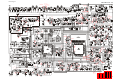
Automatic Transmit Power Control
Current from the final amplifier is sampled by R1108,
R1115, and R1125, and is rectified by Q1057 (IMZ2A
T108). The resulting DC is fed back through Q1032
(FMW1 T98) to the drive amplifier Q1016 and final am-
plifier Q1024, for control of the power output.
The microprocessor selects “High” or “Low” power levels.
Transmit Inhibit
When the transmit PLL is unlocked, pin 7 of PLL chip
Q1005 goes to a logic “Low,” and unlock detector Q1056
(2SA1586Y TE85R) goes to a logic “High.” The result-
ing DC unlock control voltage is passed to pin 14 of the
microprocessor, Q1014. While the transmit PLL is un-
locked, pin 22 of Q1014 remains high, which then turns
off Q1029 (CPH6102-TL) and the Automatic Power Con-
troller Q1032 (FMW1 T98) to disable the supply voltage
to the drive amplifiers Q1015/Q1016 and final amplifier
Q1024, thereby disabling the transmitter.
Spurious Suppression
Generation of spurious products by the transmitter is
minimized by the fundamental carrier frequency being
equal to final transmitting frequency, modulated directly
in the transmit VCO. Additional harmonic suppression is
provided by a low-pass filter consisting of coils L1001,
L1002, and L1031 plus capacitors C1004, C1005, C1008,
C1010, C1014, C1016, and C1221, resulting in more than
60 dB of harmonic suppression prior to delivery of the RF
signal to the antenna.
PLL Frequency Synthesizer
The PLL circuitry on the Main Unit consists of VCO
Q1002 (2SC5231C8-TL), VCO buffer Q1007
(2SC5005), and PLL subsystem IC Q1005
(MB15A02PFV1-G-BND-EF), which contains a refer-
ence divider, serial-to-parallel data latch, programmable
divider, phase comparator, and charge pump.
Frequency stability is maintained by temperature com-
pensating thermistor TH1004. The output from TH1004
is applied to pin 39 of Q1014. Q1014 outputs thermal data
to D/A converter Q1052 (M62364FP 600D), which pro-
duces a DC voltage corresponding to the thermal data.
The resulting DC voltage is applied to varactor diode
D1004 (HVC350B TRF) to stabilize the 14.60 MHz Ref-
erence Frequency.
While receiving, VCO Q1002 oscillates between
190.25 and 218.25 MHz according to the transceiver ver-
sion and the programmed receiving frequency. The VCO
output is buffered by Q1007, then applied to the prescaler
section of Q1005. There the VCO signal is divided by 64
or 65, according to a control signal from the data latch
section of Q1005, before being sent to the programmable
divider section of Q1005.
The data latch section of Q1005 also receives serial
dividing data from the microprocessor, Q1014, which
causes the pre-divided VCO signal to be further divided
in the programmable divider section, depending upon the
desired receive frequency, so as to produce a 2.5 kHz or
3.125 kHz derivative of the current VCO frequency.
Meanwhile, the reference divider section of Q1005
divides the 14.60 MHz crystal reference (from the refer-
ence oscillator, Q1022) by 5840 (or 4672) to produce the
2.5 kHz (or 3.125 kHz) loop references (respectively).
The 2.5 kHz (or 3.125 kHz) signal from the program-
mable divider (derived from the VCO) and that derived
from the reference oscillator are applied to the phase de-
tector section of Q1004, which produces a pulsed output
with pulse duration depending on the phase difference
between the input signals.
This pulse train is filtered to DC and returned to the
varactor D1037 and D1042 (both, typ A, C:HVC358B or
typ CS1:1SV305). Changes in the level of the DC volt-
age are applied to the varactor, affecting the reference in
the tank circuit of the VCO according to the phase differ-
ence between the signals derived from the VCO and the
crystal reference oscillator.
The VCO is thus phase-locked to the crystal reference
oscillator. The output of the VCO Q1002, after buffering
by Q1007, is applied to the first mixer as described previ-
ously.
For transmission, the VCO Q1002 oscillates between
146 and 174 MHz according to the model version and
programmed transmit frequency. The remainder of the PLL
circuitry is shared with the receiver. However, the divid-
ing data from the microprocessor is such that the VCO
frequency is at the actual transmit frequency (rather than
offset for IFs, as in the receiving case). Also, the VCO is
modulated by the speech audio applied to D1005 (typ
A:HVU358 TRF, typ C:1SV229 TPH3, typ
CS1:1SV229 TPH3:Lot. 45~, HVU358 TRF:Lot. 54~),
as described previously.
Receive and transmit buses select which VCO is made
active, using Q1059 and Q1063 (both RT1P441U-T11-
1).
Miscellaneous Circuits
Push-To-Talk Transmit Activation
The PTT switch on the microphone is connected to pin
48 of microprocessor Q1014, so that when the PTT switch
is closed, pin 23 of Q1014 goes low. This signal disables
the receiver by disabling the 5 V supply bus at Q1036
(DTB123EK T146) to the front-end, FM IF subsystem
IC Q1037, and the receiver VCO circuitry.
At the same time, Q1027 (FMW1 T98) and Q1029
(CPH6102-TL) activate the transmit 5V supply line to
enable the transmitter.
Circuit Description