VERTEX STANDARD CO., LTD. 4-8-8 Nakameguro, Meguro-Ku, Tokyo 153-8644, Japan VERTEX STANDARD VHF Land Mobile Transceiver US Headquarters 10900 Walker Street, Cypress, CA 90630, U.S.A. International Division 8350 N.W. 52nd Terrace, Suite 201, Miami, FL 33166, U.S.A. VX-2000V YAESU EUROPE B.V. P.O. Box 75525, 1118 ZN Schiphol, The Netherlands Service Manual ©2003 VERTEX STANDARD CO., LTD. YAESU UK LTD. Unit 12, Sun Valley Business Park, Winnall Close Winchester, Hampshire, SO23 0LB, U.K.
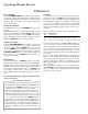
Operating Manual Reprint CONTROLS & CONNECTORS 4 channel version À Microphone Jack Connect the microphone plug to this jack. Á MONI Button & Indicator This button selects the “squelch” (receiver mute) mode. When the yellow indicator is off, “tone” or “coded” squelch is active. When the indicator glows steadily, only “noise squelch” is active, and any signal present on the channel will be heard.
Operating Manual Reprint REAR (Heatsink) À 13.6V DC Cable Pigtail w/Connector The supplied DC power cable must be affixed to this 2-pin connector. Á Antenna Socket The 50-ohm coaxial feedline to the antenna must be connected here, using a “UHF” type (PL-259) plug. Â External Speaker Jack An external loudspeaker may be connected to this 2-contact, 3.5-mm miniature phone jack.
Operating Manual Reprint OPERATION Power ON/OFF Scanning Turn the VOLUME/POWER knob clockwise to turn on the radio. The active display and channel indicators will become illuminated, indicating the status of the radio. The channel indicated will be the same one on which you were operating when the radio was last turned off. To activate scanning on your radio, first place the microphone in its hanger. Now press the SCAN button momentarily.
Operating Manual Reprint USER PROGRAMMABLE CHANNEL SELECTIONS You can program a list of channels to be scanned, and up to two channels to be monitored on a “priority” basis. Your selections will be maintained in memory until you change or delete them. Setting of these channels involves two small “Dot” indicators at the top of the channel display field.
Operating Manual Reprint J1003 DSUB 9-Pin Data Connector Pin Assignment Ä Ã Â Á À È Ç Æ Å À SQ: Squelch Signal Output Carrier In: Active High (5 V / 47 kΩ) Á RX_AUD_OUT: Received Audio Output (Two choices available) Á-1 De-Empasized Audio Output: 100 mV / 10 kΩ This output level's default state is fixed at the factory by having no jumper at JP1003 and soldering the jumper at JP1002 on the MAIN Unit.
Specifications General Frequency Range (version): No. of Channels & Spacing: Modes of Emission: Frequency Stability: Antenna Requirements: Voltage Requirements: Current Consumption (approx.): Operating Temperature Range: Size (WHD, approx.): Weight (approx.): 134 ~160 or 148 ~ 174 MHz (VHF vers. A/C, respectively) 4 or 40 channels 25-kHz, 12.5-kHz spacing 16K0F3E ,11K0F3E ±0.00025% 50 ohms, unbalanced (SO-239 socket) 11.8 V to 15.6 V DC, negative ground 250 mA Stby, 200 mA Rx, 6.
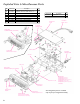
Exploded View & Miscellaneous Parts REF. À Á Â Ã Ä Å Æ VXSTD P/N U24208001 U20208001 U20306002 U23205001 U23206001 U24306002 U31206007 U24308001 Description TAPTITE SCREW M2.6X8 (Lot. 1~5) BINDING HEAD SCREW M2.6X8 (Lot. 6~) BINDING HEAD SCREW M3X6NI TAPTITE SCREW M2.6X5 TAPTITE SCREW M2.6X6 TAPTITE SCREW M3X6NI OVAL HEAD SCREW M2.6X6B TAPTITE SCREW M3X8 Qty. 1 1 4 4 3 5 7 1 VXSTD P/N Q0000062 Description FUSE 10A T9021810 DC CABLE Qty.
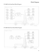
Block Diagram VX-2000V 4ch Front Panel Block Diagram VX-2000V 40ch Front Panel Block Diagram 9
Block Diagram Note: 10
Block Diagram VX-2000V Main Unit Block Diagram 11
Block Diagram Note: 12
Interconnection Diagram (T9206689A: Lot 7~) VX-2000V 4ch Front Interconnection Diagram 13
Interconnection Diagram (T9206689A: Lot 7~) VX-2000V 40ch Front Interconnection Diagram 14
Circuit Description Receive Signal Path Incoming RF energy from the antenna jack is delivered to the MAIN Unit, and passes through a low-pass filter consisting of coils L1001, L1002, L1004, and L1006, capacitors C1002, C1006, C1009, C1017, C1019, C1022, C1041, and C1046, and switching diodes D1002 (UM9957F) and D1006 (RLS135), then delivered to the receiver front end.
Circuit Description When a carrier appears at the discriminator, noise is removed from the output, causing pin 33 of Q1039 to go "high," in turn causing the "BUSY" LED and audio output lines to turn on. The microprocessor then checks for CTCSS information. If CTCSS decode is not activated, or if CTCSS decode is activated and a signal carrying a matching tone is received, the microprocessor allows audio to pass through AF mute gate Q1008 and audio amplifier Q1003 to the speaker.
Circuit Description (2SB1201STP-FA), Q1040 (2SC4116GR), and D1029 (02CZ5.6Y), with temperature compensation provided by thermistors TH1003/TH1004 and capacitors associated with the 17.25 MHz reference crystal, X1002. In the receive mode, VCO Q1046 oscillates between 130.3 and 156.3 MHz, according to the transceiver version and the programmed receiving frequency. The VCO output is buffered by Q1044, and applied to the prescaler section of Q1050.
Circuit Description Channel Selection & Display (4-channel version) Channel Selection & Display (40-channel version) The CHANNEL button on the front panel causes microprocessor Q1039 to select the operating frequency and CTCSS frequency data from serial EEPROM Q1049 (BR93LC66RF). The operating frequency data is in the form of PLL dividing ratios, which are passed to the PLL IC on the MAIN Unit via strobe, data, and clock outputs on pins 43, 42, and 41 respectively.
Alignment The VX-2000 is carefully aligned at the factory for the specified performance across the designed frequency range. Realignment should, therefore, not be necessary except in the event of a component failure, or when altering the frequency range (“version”). The following procedures cover the sometimescritical and tedious adjustments that are not normally required once the transceiver has left the factory.
Alignment Alignment Preparation & Precautions Before beginning alignment, connect the transceiver to the PC using the VPL-1 Connection Cable, and upload the current frequency data from the customer’s radio to the computer; save this information to disk so that it can be downloaded to the radio again after alignment is completed.
Alignment Now select channel 1, and confirm that the reading changes to about 1.0V for Version A, or 0.8V for Version C. r Again select channel 3. Key the transmitter, and confirm that the voltmeter reading is approximately 4.5V. r Once more select channel 1 and again key the transmitter. Confirm that the voltmeter reading is approximately 1.0V for Version A, and at least 1.0V for Version C.
Alignment able DCS code 627 (encode), and download this data to the transceiver. r With the AF generator still set to zero, key the transmitter, and adjust VR1005 (MAIN Unit) for ±900 Hz deviation on the DCS signal (within 100 Hz). Receiver Squelch Threshold r Set the transceiver to channel 2. Set the RF sig- nal generator to the same frequency (147.000 for version A, 161.000 MHz for version C). Set the signal generator’s output to -8 dBµ.
MAIN Unit (Lot. 1~) Circuit Diagram 13.5 (12.8) 0 (7.0) 13.8 (13.5) 3.4 (4.0) 0 (2.1) 13.5 (7.5) 0 (1.9) 7.1 (7.0) 7.5 (7.4) 2.8 0 (4.3) (4.0) 2.9 (2.1) 0 (8.4) 0 (5.1) 0 (1.2) 5.6 (5.5) 0 (6.7) 4.9 (5.0) 0.7 (0) 2.9 (4.3) 6.1 (0) 0.1 (0.7) 3.4 (0) 0 (1.6) 5.6 (0.1) 13.8 (13.8) 0 (4.7) 1.5 (0.1) 0.98VP-P 3.9 (4.0) 0.13VP-P 0.8 (-0.2) 4.7 (0) 13.8 (13.5) 2.0 (2.2) 2.6 (2.7) 2.6 (2.7) 0.46VP-P 0.6 (0) 4.0 (4.0) 0.6 (0) 4.4 (4.4) 5.0 (0.1) 6.4 (0.1) 6.5 (0.1) 0 (0) 2.6 (2.5) 2.
MAIN Unit (Lot.
MAIN Unit (Lot. 1~) Parts Layout A B C D E F G H 1 MB89P677ARFM (Lot. 1~) MB89677ARPFM (Lot. 2~) (Q1039) MX165BDW (Q1009) SC370651FR2 (Q1050) BA4116FV (Q1029) 2 NJM2902V (Q1007, 1016) NJM2904V (Q1017) 3 TDA2003H (Q1003) 2SB1143S (Q1014) 4 Side A HA17805P (Q1010) MA143 (MC) (D1017) DAP202U (P) (D1016, 1037) KV1470 (F7) (D1007, 1008) DTC124EU (25) (Q1053) (Q1048: Lot.
MAIN Unit (Lot. 1~) A B C D E F G H 1 2 3 4 Side B M67741H-01 (Q1011) MM1216ENRE (1A) (Q1001) 26 BR93LC66RF (Q1049) AN8005M (Q1030) IMH6 (H6) (Q1004, 1025, 1052) 2SC3357 (RK) (Q1028) DTB123EK (F12) (Q1006) DTC124EU (25) (Q1020, 1033, 1051) DTB123YK (F56) (Q1005: Lot. 1~) DTB113ZK (G11) (Q1005: Lot. 4~) 2SC4116GR (LG) (Q1040, 1045, 1047) 2SC5107O (MFO) (Q1038, 1041) 2SA1586Y (SY) (Q1032, 1034) HZM7C (24) (Lot.
MAIN Unit (Lot.
MAIN Unit (Lot.
MAIN Unit (Lot. 5~) Parts Layout A B C D E F G H 1 MB89P677ARFM (Lot. 1~) MB89677ARPFM (Lot. 2~) (Q1039) MX165BDW (Lot. 1~) MX165CDW (Lot. 6~) (Q1009) SC370651FR2 (Q1050) BA4116FV (Lot. 1~) TA31136FN (Lot. 7~) (Q1029) 2 NJM2902V (Q1007, 1016) NJM2904V (Q1017) 3 TDA2003H (Q1003) 2SB1143S (Q1014) 4 Side A HA17805P (Q1010) MA143 (MC) (D1017) DAP202U (P) (D1016, 1037) KV1470 (F7) (D1007, 1008) DTC124EU (25) (Q1053) (Q1048: Lot. 1) 2SC3357 (RK) (Q1031) SGM2016M (M-) (Lot.
MAIN Unit (Lot. 5~) A B C D E F G H 1 2 3 4 Side B M67741H-01 M67741L-01 (Ver A: Lot. 6~) (Q1011) MM1216ENRE (1A) (Q1001) 30 BR93LC66RF (Q1049) AN8005M (Q1030) IMH6 (H6) (Q1004, 1025, 1052) 2SC3357 (RK) (Q1028) DTB123EK (F12) (Q1006) DTC124EU (25) (Q1020, 1033, 1051) DTB123YK (F56) (Q1005: Lot. 1~) DTB113ZK (G11) (Q1005: Lot. 4~) 2SC4116GR (LG) (Q1040, 1045, 1047) 2SC5107O (MFO) (Q1038, 1041) 2SA1586Y (SY) (Q1032, 1034) HZM7C (24) (Lot.
MAIN Unit (Lot.
MAIN Unit (Lot.
MAIN Unit (Lot. 19~) Parts Layout A B C D E F G H 1 MB89P677ARFM (Lot. 1~) MB89677ARPFM (Lot. 2~) MB89P677APFM (NTL: Lot. 53~) MB89677ARPFM (EXP, STANDARD, VTX: Lot. 53~) (Q1039) 2 SC370651FR2 MC145192FR2 (Lot. 26~) MC145193FR2 (Lot. 41~) (Q1050) BA4116FV TA31136FN (Lot. 7~) (Q1029) 3 4 MX165BDW MX165CDW (Lot. 6~) (Q1009) NJM2902V (Q1007, 1016) NJM2904V (Q1017) Side A 2SB1201STP (Q1002) TDA2003H (Q1003) MA143 (MC) (D1017) DAP202U (P) (D1016, 1037) KV1470 (F7) KV1870STL (Lot.
MAIN Unit (Lot. 19~) A B C D E F G H 1 2 3 4 Side B M67741H-01 (Q1011) MM1216ENRE (1A) (Q1001) 34 BR93LC66RF BR93L66RF (Lot. 85~) (Q1049) AN8005M (Q1030) IMH6 (H6) (Q1004, 1025, 1052) 2SC3357 (RK) (Q1028) DTB123EK (F12) (Q1006) DTC124EU (25) (Q1020, 1033, 1051) DTB123YK (F56) (Q1005: Lot. 1~) DTB113ZK (G11) (Q1005: Lot. 4~) 2SC4116GR (LG) (Q1040, 1045, 1047) 2SC5107O (MFO) (Q1038, 1041) 2SA1586Y (SY) (Q1032, 1034) HZM7C (24) (Lot. 2~62) (D1024) DTC323TK (H02) (Q1008) HZM7.
MAIN Unit Parts List REF. DESCRIPTION VALUE WV TOL. MFR’S DESIG VXSTD P/N VERS. LOT. SIDE. LAY ADR.
MAIN Unit REF. C 1041 C 1042 C 1044 C 1045 C 1046 C 1046 C 1046 C 1047 C 1048 C 1049 C 1049 C 1050 C 1051 C 1052 C 1052 C 1052 C 1053 C 1053 C 1053 C 1054 C 1054 C 1054 C 1054 C 1055 C 1056 C 1057 C 1057 C 1057 C 1058 C 1058 C 1058 C 1058 C 1059 C 1060 C 1061 C 1062 C 1063 C 1065 C 1066 C 1067 C 1067 C 1068 C 1069 C 1069 C 1069 C 1070 C 1071 C 1071 C 1072 C 1073 C 1073 C 1073 C 1073 C 1074 C 1075 C 1076 C 1078 C 1079 C 1080 C 1081 36 DESCRIPTION VALUE WV CHIP CAP. CHIP CAP. CHIP CAP. CHIP CAP.
MAIN Unit REF. C 1082 C 1083 C 1084 C 1085 C 1086 C 1087 C 1089 C 1091 C 1091 C 1091 C 1091 C 1092 C 1092 C 1092 C 1093 C 1093 C 1093 C 1094 C 1094 C 1094 C 1095 C 1096 C 1096 C 1096 C 1098 C 1099 C 1100 C 1100 C 1100 C 1101 C 1101 C 1101 C 1103 C 1104 C 1105 C 1105 C 1105 C 1106 C 1106 C 1106 C 1107 C 1108 C 1109 C 1109 C 1109 C 1109 C 1110 C 1110 C 1110 C 1112 C 1113 C 1114 C 1115 C 1116 C 1117 C 1118 C 1119 C 1120 C 1121 C 1122 DESCRIPTION VALUE CHIP CAP. AL.ELECTRO.CAP. CHIP CAP. CHIP CAP. CHIP CAP.
MAIN Unit REF. C 1123 C 1124 C 1125 C 1126 C 1127 C 1128 C 1129 C 1130 C 1131 C 1132 C 1133 C 1134 C 1134 C 1134 C 1134 C 1135 C 1136 C 1137 C 1138 C 1139 C 1140 C 1141 C 1142 C 1143 C 1144 C 1145 C 1146 C 1147 C 1148 C 1151 C 1151 C 1151 C 1153 C 1154 C 1155 C 1156 C 1157 C 1158 C 1159 C 1160 C 1161 C 1162 C 1163 C 1164 C 1165 C 1166 C 1167 C 1168 C 1169 C 1170 C 1171 C 1172 C 1173 C 1174 C 1175 C 1176 C 1177 C 1178 C 1179 C 1180 38 DESCRIPTION CHIP CAP. CHIP CAP. CHIP CAP. CHIP CAP. CHIP CAP. CHIP CAP.
MAIN Unit REF. C 1181 C 1182 C 1183 C 1184 C 1185 C 1186 C 1187 C 1188 C 1189 C 1190 C 1191 C 1192 C 1193 C 1194 C 1195 C 1196 C 1197 C 1198 C 1199 C 1200 C 1201 C 1201 C 1201 C 1201 C 1201 C 1202 C 1203 C 1204 C 1205 C 1206 C 1206 C 1206 C 1207 C 1208 C 1209 C 1210 C 1211 C 1211 C 1211 C 1212 C 1213 C 1214 C 1215 C 1216 C 1217 C 1218 C 1219 C 1220 C 1221 C 1222 C 1223 C 1224 C 1225 C 1226 C 1227 C 1228 C 1229 C 1230 C 1231 C 1232 DESCRIPTION CHIP CAP. CHIP CAP. CHIP CAP. CHIP CAP. CHIP CAP. CHIP CAP.
MAIN Unit REF. DESCRIPTION C 1234 CHIP CAP. C 1235 CHIP CAP. C 1236 CHIP CAP. C 1237 CHIP TA.CAP. C 1238 CHIP CAP. C 1239 CHIP CAP. C 1240 CHIP CAP. C 1241 CHIP CAP. C 1242 CHIP CAP. C 1243 CHIP CAP. C 1244 CHIP CAP. C 1245 CHIP CAP. C 1246 CHIP CAP. C 1247 CHIP CAP. C 1248 AL.ELECTRO.CAP. C 1249 CHIP CAP. C 1250 CHIP CAP. C 1250 CHIP CAP. C 1251 CHIP CAP. C 1252 CHIP TA.CAP. C 1254 CHIP CAP. C 1254 CHIP CAP. C 1255 CHIP CAP. C 1256 CHIP CAP. C 1256 CHIP TA.CAP. C 1257 CHIP TA.CAP. C 1258 CHIP CAP.
MAIN Unit REF.
MAIN Unit LOT. REF. L 1013 L 1014 L 1015 L 1015 L 1015 L 1016 L 1016 L 1016 L 1017 L 1018 L 1019 L 1020 L 1021 L 1021 L 1024 L 1025 L 1026 L 1027 L 1028 L 1029 L 1030 L 1031 L 1031 L 1031 L 1032 L 1032 L 1032 L 1033 Q 1001 Q 1002 Q 1003 Q 1004 Q 1005 Q 1005 Q 1006 Q 1007 Q 1008 Q 1009 Q 1009 Q 1010 Q 1010 Q 1011 Q 1011 Q 1011 Q 1012 Q 1014 Q 1015 Q 1016 Q 1017 Q 1020 Q 1021 Q 1021 Q 1022 Q 1025 Q 1026 Q 1028 Q 1029 Q 1029 Q 1030 Q 1031 42 DESCRIPTION COIL COIL M.RFC M.RFC M.RFC M.RFC M.RFC M.RFC M.RFC M.
MAIN Unit REF.
MAIN Unit REF. R 1027 R 1028 R 1029 R 1030 R 1031 R 1032 R 1033 R 1034 R 1035 R 1036 R 1037 R 1038 R 1039 R 1039 R 1042 R 1042 R 1043 R 1043 R 1043 R 1043 R 1044 R 1045 R 1046 R 1046 R 1046 R 1046 R 1047 R 1047 R 1047 R 1047 R 1048 R 1049 R 1050 R 1052 R 1053 R 1054 R 1055 R 1056 R 1057 R 1058 R 1059 R 1060 R 1062 R 1063 R 1064 R 1065 R 1066 R 1067 R 1068 R 1069 R 1069 R 1070 R 1071 R 1072 R 1072 R 1073 R 1074 R 1075 R 1076 R 1077 44 DESCRIPTION CHIP RES. CHIP RES. CHIP RES. CHIP RES. CHIP RES. CHIP RES.
MAIN Unit REF. R 1078 R 1079 R 1080 R 1081 R 1082 R 1083 R 1085 R 1086 R 1087 R 1088 R 1089 R 1090 R 1091 R 1092 R 1093 R 1094 R 1095 R 1096 R 1097 R 1098 R 1099 R 1100 R 1101 R 1102 R 1103 R 1104 R 1105 R 1106 R 1107 R 1108 R 1109 R 1109 R 1109 R 1109 R 1110 R 1111 R 1112 R 1113 R 1114 R 1115 R 1115 R 1116 R 1117 R 1118 R 1119 R 1120 R 1120 R 1121 R 1122 R 1123 R 1123 R 1124 R 1125 R 1126 R 1128 R 1129 R 1130 R 1131 R 1132 R 1133 DESCRIPTION CHIP RES. CHIP RES. CHIP RES. CHIP RES. CHIP RES. CHIP RES.
MAIN Unit REF. R 1134 R 1135 R 1135 R 1136 R 1137 R 1138 R 1138 R 1139 R 1139 R 1140 R 1141 R 1142 R 1143 R 1144 R 1145 R 1146 R 1147 R 1148 R 1149 R 1150 R 1151 R 1151 R 1152 R 1153 R 1154 R 1155 R 1157 R 1158 R 1159 R 1160 R 1161 R 1162 R 1163 R 1164 R 1165 R 1166 R 1167 R 1168 R 1169 R 1170 R 1171 R 1172 R 1173 R 1174 R 1175 R 1176 R 1177 R 1178 R 1179 R 1180 R 1181 R 1182 R 1182 R 1182 R 1182 R 1183 R 1184 R 1185 R 1185 R 1186 46 DESCRIPTION CHIP RES. CHIP RES. CHIP RES. CHIP RES. CHIP RES. CHIP RES.
MAIN Unit REF. R 1187 R 1188 R 1188 R 1189 R 1190 R 1190 R 1191 R 1192 R 1193 R 1194 R 1195 R 1196 R 1197 R 1198 R 1199 R 1200 R 1201 R 1202 R 1203 R 1204 R 1205 R 1206 R 1207 R 1208 R 1209 R 1210 R 1211 R 1212 R 1213 R 1214 R 1215 R 1215 R 1216 R 1217 R 1218 R 1219 R 1220 R 1221 R 1222 R 1223 R 1224 R 1225 R 1226 R 1226 R 1226 R 1227 R 1228 R 1229 R 1230 R 1231 R 1232 R 1233 R 1234 R 1235 R 1236 R 1237 R 1238 R 1238 R 1238 R 1239 DESCRIPTION CHIP RES. CHIP RES. CHIP RES. CHIP RES. CHIP RES. CHIP RES.
MAIN Unit REF. R 1240 R 1241 R 1242 R 1243 R 1244 R 1245 R 1246 R 1246 R 1247 R 1247 R 1248 R 1249 R 1250 R 1250 R 1250 R 1251 R 1251 R 1251 R 1253 R 1254 R 1255 R 1255 R 1256 R 1257 R 1257 R 1258 R 1258 R 1259 R 1260 R 1261 R 1262 R 1263 T 1001 T 1002 TC1001 TH1001 TH1003 TH1004 VR1001 VR1002 VR1003 VR1004 VR1005 VR1006 X 1001 X 1002 XF1001 XF1002 48 DESCRIPTION CHIP RES. CHIP RES. CHIP RES. CHIP RES. CHIP RES. CHIP RES. CHIP RES. CHIP RES. CHIP RES. CHIP RES. CHIP RES. CHIP RES. CHIP RES. CHIP RES.
Display-1 Unit Circuit Diagram 49
Display-1 Unit Parts Layout Side A Side B BU4094BCFV (Q2002) 50 XN1213 (9L) (Q2001, 2003, 2004) DTC124EK (25) (Q2005)
Display-1 Unit Parts List REF. DESCRIPTION VALUE WV TOL. MFR’S DESIG VXSTD P/N VERS. LOT. SIDE. LAY ADR. *** DISPLAY-1 UNIT *** D 2001 D 2002 D 2003 D 2004 D 2005 D 2006 D 2007 D 2008 D 2009 JP2001 Q 2001 Q 2002 Q 2002 Q 2003 Q 2004 Q 2005 R 2001 R 2002 R 2003 R 2004 R 2005 R 2006 R 2007 R 2008 R 2009 PCB with Components Printed Circuit Board LED LED LED LED LED LED LED DIODE DIODE WIRE ASSY TRANSISTOR IC IC TRANSISTOR TRANSISTOR TRANSISTOR CHIP RES. CHIP RES. CHIP RES. CHIP RES. CHIP RES.
Display-1 Unit Note: 52
Display-2 Unit Circuit Diagram 53
Display-2 Unit Parts Layout Side A Side B DN8657S (Q3001) DTC124EK (25) (Q3003) 9 1 D.P2 C2 Dig.1 E2 B2 C1 54 E1 G1 F2 A2 Dig.2 D1 G2 10 13 D.
Display-2 Unit Parts List REF. DESCRIPTION VALUE WV TOL. MFR’S DESIG VXSTD P/N VERS. LOT. SIDE. LAY ADR. *** DISPLAY-2 UNIT *** D 3002 D 3003 D 3004 D 3005 D 3006 D 3007 D 3008 DS3001 JP3001 Q 3001 Q 3002 Q 3003 R 3001 R 3002 R 3003 R 3004 R 3005 PCB with Components Printed Circuit Board DIODE LED DIODE DIODE LED DIODE LED LED WIRE ASSY IC TRANSISTOR TRANSISTOR CHIP RES. CHIP RES. CHIP RES. CHIP RES. CHIP RES.
Display-2 Unit Note: 56
VR Unit Circuit Diagram Parts Layout Side A Side B Parts List REF. DESCRIPTION VALUE WV TOL. MFR’S DESIG VXSTD P/N VERS. LOT. SIDE. LAY ADR. *** VR UNIT *** PCB with Components Printed Circuit Board VR4001 POT.
MIC Unit Circuit Diagram Parts Layout Side A Side B Parts List REF. DESCRIPTION VALUE WV TOL. MFR’S DESIG VXSTD P/N VERS. LOT. SIDE. LAY ADR.
No portion of this manual may be reproduced without the ermission of VERTEX STANDARD CO., LTD. Copyright © 2003 VERTEX STANDARD CO., LTD.