
User`s manual


Chapter 3
52
FREQUENCY/VOLTAGE CONTROL
: Move
F5: Previous Values F6: Fail-Safe Defaults F7: Optimized Defaults
Enter: Select +/-/PU/PD: Value F10: Save ESC: Exit F1: General Help
Menu Level
Item Help
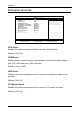
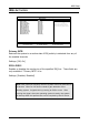
DRAM Clock [By SPD]
DRAM Timing [Auto By SPD]
Bank Interleave Disabled
Precharge to Active(Trp) 4T
Active to Precharge(Tras) 9T
Active to CMD(Trcd) 4T
REF to ACT/REF to REF(Trfc) 15T
ACT(0) to ACT(1) (TRRD) 3T
DRAM Command Rate [2T Command]
SDRAM CAS Latency 2.5
Frequency / Voltage Control
Phoenix - AwardBIOS CMOS Setup Utility
Spread Spectrum Range +/- 0.3%
Spread Spectrum [Enabled]
DRAM Clock
The chipset supports synchronous and asynchronous mode between host
clock and DRAM clock frequency.
Settings: [By SPD, 100 MHz, 133 MHz, 166 MHz, 200MHz]
DRAM Timing
The value in this field depends on the memory modules installed in your
system. Changing the value from the factory setting is not recommended
unless you install new memory that has a different performance rating than
the original modules.
Settings: [Manual, Auto By SPD]
SDRAM CAS Latency
This item is for setting the speed it takes for the memory module to complete
a command. Generally, a lower setting will improve the performance of your
system. However, if your system becomes less stable, you should change it
to a higher setting. This field is only available when “DRAM Timing” is set to
“Manual”.
Settings: [1.5, 2, 2.5, 3]