
User guide

Picor Corporation • www.picorpower.com PI2121-EVAL1 User Guide Rev 1.1 Page 2 of 12
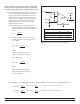
The Cool-ORing PI2121 is a complete full-function Active
ORing solution with a high-speed ORing MOSFET controller
and a very low on-state resistance MOSFET designed for use
in redundant power system architectures. The PI2121 Cool-
ORing solution is offered in an extremely small, thermally
enhanced 5 mm x 7 mm LGA package and can be used in low
voltage (≤ 5 Vbus) high side Active ORing applications. The
PI2121 enables extremely low power loss with fast dynamic
response to fault conditions, critical for high availability
systems. A master / slave feature allows the paralleling of
PI2121 solutions for high current Active ORing requirements.
The PI2121, with its 1.5 mΩ internal MOSFET provides very
high efficiency and low power loss during steady state
operation, while achieving high-speed turn-off of the internal
MOSFET during input power source fault conditions that
cause reverse current flow. The PI2121 provides an active low
fault flag output to the system during excessive forward
current, light load, reverse current, over-voltage,
under-voltage, and over-temperature fault conditions.
A temperature sensing function indicates a fault if the
maximum junction temperature exceeds 160°C. The
under-voltage and over-voltage thresholds are programmable
via an external resistor divider.
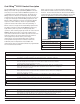
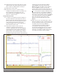
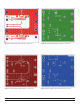
Figure 1 shows a photo of the PI2121-EVAL1 evaluation
board, with two PI2121 used to form the two Active ORing
channels. The board is built with two identical Active ORing
circuits with options and features that enable the user to fully
explore the capabilities of the PI2121 Cool-ORing solution.
Figure 1 – PI2121-EVAL1 Evaluation Board (1.8" x 1.8")
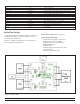
Terminals Rating
Vin1, Vin2 8V / 24 A
Vaux1, Vaux2, (R7 = R14 = 10 Ω)
-0.3 to 17.3 V / 40 mA
see Vaux section
SL -0.3 to 8.0 V / 10 mA
FT -0.3 to 17.3 V / 10 mA
Terminal Description
Vin1 Power Source Input #1 or bus input designed to accommodate up to 24 A continuous current.
Vaux1 Auxiliary Input Voltage #1 to supply PI2121 (SiP1) VC power. Vaux1 should be equal to Vin1 plus
5 V or higher. See details in Auxiliary Power Supply (Vaux) section of the PI2121 data sheet.
Rtn1 Vaux1 Return Connection: Connected to Ground plane
Gnd Vin & Vout Return Connection: Three Gnd connections are available and are connected to a common
point, the Ground plane. Input supplies Vin1 & Vin2 and the output load at Vout should all be
connected to their respective local Gnd connection.
SL1 PI2121 (SiP1) Slave Input-Output Pin: For monitoring SiP1 slave pin. When SiP1 is configured as the
Master, this pin functions as an output that drives slaved PI2121 devices. When SiP1 is configured in
Slave mode, SL1 serves as an input.
SL2 PI2121 (SiP2) Slave Input-Output Pin: For monitoring SiP2 slave pin. When SiP2 is configured as the
Master, this pin functions as an output that drives slaved PI2121 devices. When SiP2 is configured in
Slave mode, SL2 serves as an input.
Vin2 Power Source Input #2 or bus input designed to accommodate up to 24 A continuous current.
Vaux2 Auxiliary Input Voltage #2 to supply PI2121 (SiP2) VC power. Vaux2 should be equal to Vin2 plus 5 V or higher.
See details in Auxiliary Power Supply (Vaux) section of the PI2121 data sheet.
Rtn2 Vaux2 Return Connection: Connected to Ground plane
FT1 PI2121 (SiP1) Fault Pin: Monitors SiP1 fault conditions
FT2 PI2121 (SiP2) Fault Pin: Monitors SiP2 fault conditions
Vout Output: SiP1 and SiP2 D pins connection, connect to the load high side.
Table 1 – PI2121-EVAL1 Evaluation Board terminals description
Cool-ORing
TM
PI2121 Product Description
Jumper Description
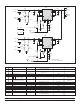
J1, J3 BK Jumpers: Connect jumper across M for master mode and across S for slave mode. Remove jumper to adjust reverse
fault blanking time using Rbk. Rbk is R6 for SiP1 and R13 for SiP2 shown in the schematic, Figure 2.
J2 Slave Jumper: Remove the jumper unless one of the PI2121 is configured in slave mode.
Table 2 – PI2121-EVAL1 Evaluation Board jumpers description