
User guide

Initial Test Set Up
To test the PI2121-EVAL1 evaluation board it is necessary to
configure the jumpers (J1, J2 and J3) first based on the
required board configuration.
Failure to configure the jumpers prior to the testing may
result in improper circuit behavior.
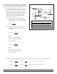
Baseline Test Procedure (Refer to Figure 3)
1.0 Recommended Equipment
1.1 Two DC power supplies - 0-10 V; 25 A.
1.2 DC power supply 12 V; 100 mA.
1.3 DC electronic load - 50 A minimum.
1.4 Digital Multimeter
1.5 Oscilloscope.
1.6 Appropriately sized interconnect cables.
1.7 Safety glasses.
1.8 PI2121 Product Data sheet.
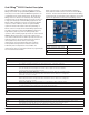
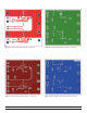
Figure 3 – Layout configuration for a typical redundant power application, using PI2121 with both solutions
configured in Master Mode.
Picor Corporation • www.picorpower.com PI2121-EVAL1 User Guide Rev 1.1 Page 4 of 12
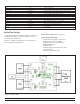
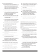
Reference Designator Value Functional Description
C1, C2 1µF VC Bypass Capacitor
C3 22µF Output (Load) Capacitor
C4, C5, C6, C7 Not installed Snubber to reduce voltage ringing when the device turns off
D1, D2 LED To indicate a fault exist when it is on
J1, J3 Jumper To select between Master and Slave Modes
J2 Jumper Connection between SL1 and SL2
R1, R8 8.45KΩ UV Voltage Divider Resistor ( R2
UV
in Figure 4)
R2, R9 13.3KΩ OV Voltage Divider Resistor ( R2
OV
in Figure 4)
R3, R10 2.00KΩ UV Voltage Divider Resistor ( R1
UV
in Figure 4)
R4, R11 2.00KΩ OV Coltage Divider Resistor ( R1
OV
in Figure 4)
R5, R12 4.99KΩ LED Current Limiter
R6, R13 Not Installed BK Delay Timer Programmable Resistor
R7, R14 10Ω VC Bias Resistor
SiP1, SiP2 PI2121 Cool ORing SiP.
Table 4 – Component functional description