
User guide

Picor Corporation • www.picorpower.com PI2121-EVAL1 User Guide Rev 1.1 Page 7 of 12
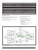
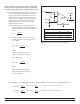
5.0 Hook Up of the Evaluation Board
5.1 OV and UV resistors values are configured for a 3.3 V
input voltage. If you are using the evaluation
board in a different input voltage level you have to
adjust the resistor values by replacing R1, R2, R8
and R9, or remove R2, R3, R9 and R10 to disable UV
and OV. Please refer to the UV/OV section for
details to set R1, R2, R8 and R9 proper values.
5.2 Verify that the jumpers J1 and J3 are installed for
master mode [across M] and no Jumper on J2.
5.3 Connect the positive terminal of PS1 power supply
to Vin1. Connect the ground terminal of PS1 to its
local Gnd. Set the power supply to 3.3 V.
Keep PS1 output disabled (OFF).
5.4 Connect the positive terminal of PS2 power supply
to Vin2. Connect the ground terminal of PS2 to its
local Gnd. Set the power supply to 3.3 V. Keep PS2
output disabled (OFF).
5.5 Connect the positive terminal of PS3 power supply
to Vaux1 and Vaux2. Connect the ground terminal
of this power supply to Rtn1 and Rtn2. Set the
power supply to 12 V. Keep PS3 output disabled (OFF).
5.6 Connect the electronic load to the output between
Vout and Gnd. Set the load current to 10 A.
5.7 Enable (turn ON) PS1 power supply output.
5.8 Turn on the electronic load.
5.9 Verify that the electronic load input voltage
reading is one diode voltage drop below 3.3 V.
5.10 Enable (turn ON) PS3 power supply output.
5.11 Verify that the electronic load voltage reading
increases to a few millivolts below 3.3 V. This
verifies that the PI2121 (SiP1) internal MOSFET is in
conduction mode.
5.12 D1 should be off. This verifies that there is no
fault condition.
5.13 Reduce PS1 output voltage to 2 V,
5.14 D1 should turn on, this verifies that the circuit is in
an under-voltage fault condition.
5.15 Increase PS1 output to 3.3 V, D1 should turn off,
then increase PS1 output to 4 V, D1 should turn on
indicating an over-voltage fault condition
5.16 Verify that Vin2 is at 0V. This verifies that the
PI2121 (SiP2) internal FET is off.
5.17 D2 should be on. This is due to a reverse voltage
fault condition caused by the bus voltage being
high with respect to the input voltage (Vin2).
5.18 Enable (turn ON) PS2 output.
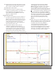
5.19 Verify that both PS1 and PS2 are sharing load
current evenly by looking at the supply current.
5.20 Disable (turn OFF) PS1, PS2 and PS3 outputs.
5.21 Enable (turn ON) PS2 output then Enable PS3 output.
5.22 Verify that the electronic load voltage reading is
few millivolts below 3.3 V. This verifies that the PI2121
(SiP2) internal MOSFET is in conduction mode.
5.23 D2 should be off. This verifies that there is no
fault condition.
5.24 Reduce PS2 output voltage to 2 V,
5.25 D2 should turn on, this verifies that the circuit is in
an under-voltage fault condition.
5.26 Increase PS2 output to 3.3 V, D2 should turn off,
then increase PS2 output to 4 V, D2 should turn on
indicating an over voltage fault condition.
5.27 Verify that Vin1 is at 0V. This verifies that the
PI2121 (SiP1) internal FET is off.
5.28 D1 should be on. This is due to a reverse voltage
fault condition caused by the bus voltage being
high with respect to the input voltage (Vin1).
6.0 Slave Mode: Slave Mode can be demonstrated in two
setups; either by using one PI2121-EVAL1 evaluation board
as a single ORing function with both PI2121 effectively in
parallel or two PI2121-EVAL1 evaluation boards to
demonstrate a true redundant 48 A system. The following
test steps uses a single PI2121-EVAL1 in a slave mode
application.
Note: In this experiment SiP 1 is configured in master mode and
SiP2 is configured in slave mode.
6.1 BK pin (J1) of the master device will be connected
to ground [across M] while the slaved device BK pin
(J3) is connected to VCC [across S]. Place a jumper
across J2 to connect slave pins together.
6.2 Connect the positive terminal of PS1 power supply
to Vin1. Connect the ground terminal of this power
supply to Gnd. Set the power supply to 3.3 V. Keep
PS1 output disabled (OFF).
6.3 Connect the positive terminal of PS2 power supply
to Vin2. Connect the ground terminal of this power
supply to Gnd. Set the power supply to 3.3 V. Keep
PS2 output disabled (OFF).
6.4 Connect the positive terminal of PS3 power supply
to Vaux1 and Vaux2. Connect the ground terminal
of this power supply to Rtn1 and Rtn2. Set the
power supply to 12 V. Keep PS3 output disabled (OFF).
6.5 Connect the electronic load between Vout and
Gnd. Set the load current to 10 A.
6.6 Enable (Turn ON) PS2, and PS3 outputs, and keep
PS1 output disabled (OFF).
6.7 Turn on the electronic load.