
Datasheet
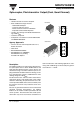
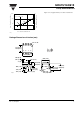

VISHAY
ILD615/ ILQ615
Document Number 83652
Rev. 1.3, 19-Apr-04
Vishay Semiconductors
www.vishay.com
3
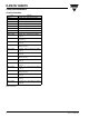
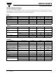
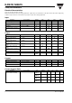
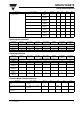
Absolute Maximum Ratings
T
amb
= 25 °C, unless otherwise specified
Stresses in excess of the absolute Maximum Ratings can cause permanent damage to the device. Functional operation of the device is
not implied at these or any other conditions in excess of those given in the operational sections of this document. Exposure to absolute
Maximum Rating for extended periods of the time can adversely affect reliability.
Input
Output
Coupler
Parameter Test condition Symbol Value Unit
Reverse voltage V
R
6.0 V
Forward current I
F
60 mA
Surge current I
FSM
1.5 A
Power dissipation P
diss
100 mW
Derate linearly from 25 °C 1.33 mW/°C
Parameter Test condition Symbol Value Unit
Collector-emitter breakdown
voltage
BV
CEO
70 V
Emitter-collector breakdown
voltage
BV
ECO
7.0 V
Collector current I
C
50 mA
t < 1.0 ms I
C
100 mA
Power dissipation P
diss
150 mW
Derate linearly from 25 °C 2.0 mW/°C
Parameter Test condition Symbol Value Unit
Storage temperature T
stg
- 55 to + 150 °C
Operating temperature T
amb
- 55 to + 100 °C
Junction temperature T
j
100 °C
Soldering temperature 2.0 mm distance from case
bottom
T
sld
260 °C
Package power dissipation,
ILD615
400 mW
Derate linearly from 25 °C 5.33 mW/°C
Package power dissipation,
ILQ615
500 mW
Derate linearly from 25 °C 6.67 mW/°C
Isolation test voltage t = 1.0 sec. V
ISO
5300 V
RMS
Creepage ≥ 7.0 mm
Clearance ≥ 7.0 mm
Isolation resistance V
IO
= 500 V, T
amb
= 25 °C R
IO
≥ 10
12
Ω
V
IO
= 500 V, T
amb
= 100 °C R
IO
≥ 10
11
Ω