
Datasheet


Document Number: 91031 www.vishay.com
S11-0509-Rev. B, 21-Mar-11 5
This datasheet is subject to change without notice.
THE PRODUCT DESCRIBED HEREIN AND THIS DATASHEET ARE SUBJECT TO SPECIFIC DISCLAIMERS, SET FORTH AT
www.vishay.com/doc?91000
IRF630, SiHF630
Vishay Siliconix
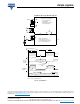
Fig. 9 - Maximum Drain Current vs. Case Temperature
Fig. 10a - Switching Time Test Circuit
Fig. 10b - Switching Time Waveforms
Fig. 11 - Maximum Effective Transient Thermal Impedance, Junction-to-Case
Fig. 12a - Unclamped Inductive Test Circuit Fig. 12b - Unclamped Inductive Waveforms
I
D
, Drain Current (A)
T
C
, Case Temperature (°C)
0
2
4
6
8
10
25 1501251007550
91031_09
Pulse width ≤ 1 µs
Duty factor ≤ 0.1 %
R
D
V
GS
R
G
D.U.T.
10 V
+
-
V
DS
V
DD
V
DS
90 %
10 %
V
GS
t
d(on)
t
r
t
d(off)
t
f
10
1
0.1
10
-2
10
-5
10
-4
10
-3
10
-2
0.1 1 10
P
DM
t
1
t
2
t
1
, Rectangular Pulse Duration (s)
Thermal Response (Z
thJC
)
Notes:
1. Duty Factor, D = t
1
/t
2
2. Peak T
j
= P
DM
x Z
thJC
+ T
C
Single Pulse
(Thermal Response)
0 − 0.5
0.2
0.1
0.05
0.02
0.01
91031_11
R
G
I
AS
0.01 Ω
t
p
D.U.T.
L
V
DS
+
-
V
DD
A
10 V
Var y t
p
to obtain
required I
AS
I
AS
V
DS
V
DD
V
DS
t
p