
Datasheet


Document Number: 91053 www.vishay.com
S11-0507-Rev. B, 21-Mar-11 1
This datasheet is subject to change without notice.
THE PRODUCT DESCRIBED HEREIN AND THIS DATASHEET ARE SUBJECT TO SPECIFIC DISCLAIMERS, SET FORTH AT
www.vishay.com/doc?91000
Power MOSFET
IRF740LC, SiHF740LC
Vishay Siliconix
FEATURES
• Ultra Low Gate Charge
• Reduced Gate Drive Requirement
• Enhanced 30 V V
GS
Rating
• Reduced C
iss
, C
oss
, C
rss
• Extremely High Frequency Operation
• Repetitive Avalanche Rated
• Compliant to RoHS Directive 2002/95/EC
DESCRIPTION
This new series of low charge Power MOSFETs achieve
significantly lower gate charge over conventional MOSFETs.
Utilizing the new LCDMOS technology, the device
improvements are achieved without added product cost,
allowing for reduced gate drive requirements and total
system savings. In addition, reduced switching losses and
improved efficiency are achievable in a variety of high
frequency applications. Frequencies of a few MHz at high
current are possible using the new Low Charge MOSFETs.
These device improvements combined with the proven
ruggedness and reliability that are characteristic of Power
MOSFETs ofter the designer a new standard in power
transistors for switching applications.
Notes
a. Repetitive rating; pulse width limited by maximum junction temperature (see fig. 11).
b. V
DD
= 50 V, starting T
J
= 25 °C, L = 9.1 mH, R
g
= 25 Ω, I
AS
= 10 A (see fig. 12).
c. I
SD
≤ 10 A, dI/dt ≤ 120 A/μs, V
DD
≤ V
DS
, T
J
≤ 150 °C.
d. 1.6 mm from case.
PRODUCT SUMMARY
V
DS
(V) 400
R
DS(on)
(Ω)V
GS
= 10 V 0.55
Q
g
(Max.) (nC) 39
Q
gs
(nC) 10
Q
gd
(nC) 19
Configuration Single
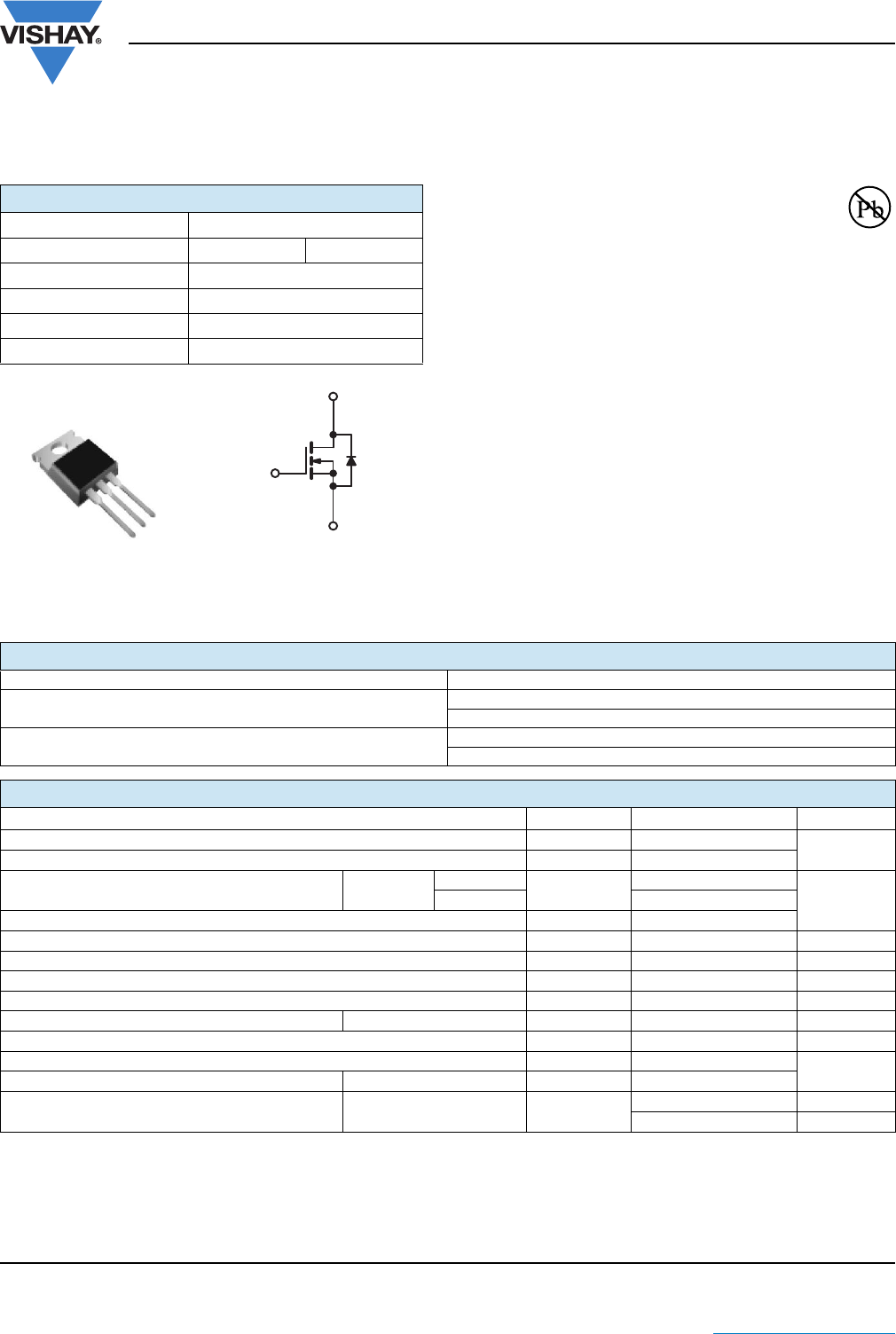
N-Channel MOSFET
G
D
S
TO-220AB
G
D
S
Available
RoHS*
COMPLIANT
ORDERING INFORMATION
Package TO-220AB
Lead (Pb)-free
IRF740LCPbF
SiHF740LC-E3
SnPb
IRF740LC
SiHF740LC
ABSOLUTE MAXIMUM RATINGS (T
C
= 25 °C, unless otherwise noted)
PARAMETER SYMBOL LIMIT UNIT
Drain-Source Voltage V
DS
400
V
Gate-Source Voltage V
GS
± 30
Continuous Drain Current V
GS
at 10 V
T
C
= 25 °C
I
D
10
A
T
C
= 100 °C 6.3
Pulsed Drain Current
a
I
DM
32
Linear Derating Factor 1.0 W/°C
Single Pulse Avalanche Energy
b
E
AS
520 mJ
Repetitive Avalanche Current
a
I
AR
10 A
Repetitive Avalanche Energy
a
E
AR
13 mJ
Maximum Power Dissipation T
C
= 25 °C P
D
125 W
Peak Diode Recovery dV/dt
c
dV/dt 4.0 V/ns
Operating Junction and Storage Temperature Range T
J
, T
stg
- 55 to + 150
°C
Soldering Recommendations (Peak Temperature) for 10 s 300
d
Mounting Torque 6-32 or M3 screw
10 lbf · in
1.1 N · m
* Pb containing terminations are not RoHS compliant, exemptions may apply