
Datasheet


KBU6A, KBU6B, KBU6D, KBU6G, KBU6J, KBU6K, KBU6M
www.vishay.com
Vishay General Semiconductor
Revision: 23-Jun-14
1
Document Number: 88657
For technical questions within your region: DiodesAmericas@vishay.com
, DiodesAsia@vishay.com, DiodesEurope@vishay.com
THIS DOCUMENT IS SUBJECT TO CHANGE WITHOUT NOTICE. THE PRODUCTS DESCRIBED HEREIN AND THIS DOCUMENT
ARE SUBJECT TO SPECIFIC DISCLAIMERS, SET FORTH AT www.vishay.com/doc?91000
Single-Phase Bridge Rectifier
FEATURES
• UL recognition, file number E54214
• Ideal for printed circuit boards
• High surge current capability
• High case dielectric strength of 1500 V
RMS
• Solder dip 275 °C max. 10 s, per JESD 22-B106
• Material categorization: for definitions of compliance
please see www.vishay.com/doc?99912
TYPICAL APPLICATIONS
General purpose use in AC/DC bridge full wave rectification
for monitor, TV, printer, SMPS, adapter, audio equipment,
and home appliances applications.
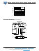
MECHANICAL DATA
Case: KBU
Molding compound meets UL 94 V-0 flammability rating
Base P/N-E4 - RoHS-compliant, commercial grade
Terminals: Silver plated leads, solderable per
J-STD-002 and JESD22-B102
Polarity: As marked on body
Mounting Torque: 10 cm-kg (8.8 inches-lbs) max.
Recommended Torque: 5.7 cm-kg (5 inches-lbs)
Notes
(1)
Recommended mounted position is to bolt down on heatsink with silicone thermal compound for maximum heat transfer with #6 screw
(2)
Thermal resistance from junction to ambient with units in free air, PCB mounted on 0.5" x 0.5" (12 mm x 12 mm) copper pads, 0.375"
(9.5 mm) lead length
(3)
Thermal resistance from junction to case with units mounted on a 2.6" x 1.4" x 0.06" thick (6.5 cm x 3.5 cm x 0.15 cm) aluminum plate
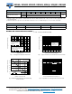
PRIMARY CHARACTERISTICS
Package KBU
I
F(AV)
6 A
V
RRM
50 V, 100 V, 200 V, 400 V, 600 V,
800 V, 1000 V
I
FSM
200 A
I
R
5 μA
V
F
at I
F
= 6 A 1.0 V
T
J
max. 150 °C
Diode variations In-Line
Case Style KBU
~
~
~
~
e4
MAXIMUM RATINGS (T
A
= 25 °C unless otherwise noted)
PARAMETER SYMBOL KBU6A KBU6B KBU6D KBU6G KBU6J KBU6K KBU6M UNIT
Maximum repetitive peak reverse voltage V
RRM
50 100 200 400 600 800 1000 V
Maximum RMS voltage V
RMS
35 70 140 280 420 560 700 V
Maximum DC blocking voltage V
DC
50 100 200 400 600 800 1000 V
Maximum average forward
rectified output current at
T
C
= 100 °C
(1)(3)
I
F(AV)
6.0
A
T
A
= 40 °C
(2)
6.0
Peak forward surge current single sine-wave
superimposed on rated load
I
FSM
250 A
Operating junction and storage temperature range T
J
, T
STG
-50 to +150 °C
ELECTRICAL CHARACTERISTICS (T
A
= 25 °C unless otherwise noted)
PARAMETER TEST CONDITIONS SYMBOL KBU6A KBU6B KBU6D KBU6G KBU6J KBU6K KBU6M UNIT
Maximum instantaneous
forward drop per diode
I
F
= 6.0 A V
F
1.0 V
Maximum DC reverse
current at rated DC blocking
voltage per diode
T
A
= 25 °C
I
R
5.0 μA
T
A
= 125 °C 1.0 mA