
Datasheet


Vishay Siliconix
Si5853DDC
Document Number: 68979
S10-0548-Rev. B, 08-Mar-10
www.vishay.com
1
P-Channel 20 V (D-S) MOSFET with Schottky Diode
FEATURES
• Halogen-free According to IEC 61249-2-21
Definition
• LITTLE FOOT
®
Plus Schottky Power MOSFET
• Compliant to RoHS Directive 2002/95/EC
APPLICATIONS
• Charging Switch for Portable Devices
- With Integrated Low V
f
Trench Schottky Diode
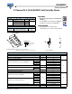
MOSFET PRODUCT SUMMARY
V
DS
(V) R
DS(on)
(Ω)I
D
(A) Q
g
(Typ.)
- 20
0.105 at V
GS
= - 4.5 V
- 4
a
4.7 nC
0.143 at V
GS
= - 2.5 V
- 3.8
0.188 at V
GS
= - 1.8 V
- 3
SCHOTTKY PRODUCT SUMMARY
V
KA
(V)
V
f
(V)
Diode Forward Voltage
I
F
(A)
20 0.46 at 0.5 A 1
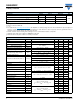
Bottom View
1206-8 ChipFET
®
A
A
S
G
K
K
D
D
1
Marking Code
JH XX
Lot Traceability
and Date Code
Part # Code
Ordering Information: Si5853DDC-T1-E3 (Lead (Pb)-free)
Si5853DDC-T1-GE3 (Lead (Pb)-free and Halogen-free)
K
A
S
G
D
P-Channel MOSFET
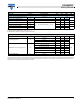
ABSOLUTE MAXIMUM RATINGS T
A
= 25 °C, unless otherwise noted
Parameter Symbol Limit Unit
Drain-Source Voltage (MOSFET) V
DS
- 20
VReverse Voltage (Schottky) V
KA
20
Gate-Source Voltage (MOSFET) V
GS
± 8
Continuous Drain Current (T
J
= 150 °C) (MOSFET)
T
C
= 25 °C
I
D
- 4
a
A
T
C
= 70 °C
- 3.5
T
A
= 25 °C
- 2.9
b, c
T
A
= 70 °C
- 2.3
b, c
Pulsed Drain Current (MOSFET) I
DM
- 10
Continuous Source Current (MOSFET Diode Conduction)
T
C
= 25 °C
I
S
- 2.6
T
A
= 25 °C
- 1.1
b, c
Average Forward Current (Schottky) I
F
1
Pulsed Forward Current (Schottky) I
FM
3
Maximum Power Dissipation (MOSFET)
T
C
= 25 °C
P
D
3.1
W
T
C
= 70 °C 2
T
A
= 25 °C
1.3
b, c
T
A
= 70 °C
0.8
b, c
Maximum Power Dissipation (Schottky)
T
C
= 25 °C 2.5
T
C
= 70 °C 1.6
T
A
= 25 °C 1.2
T
A
= 70 °C 0.76
Operating Junction and Storage Temperature Range
T
J
, T
stg
- 55 to 150
°C
Soldering Recommendation (Peak Temperature)
d, e
260