
Datasheet

Vishay Siliconix
Si7415DN
Document Number: 71691
S-83043-Rev. E, 22-Dec-08
www.vishay.com
1
P-Channel 60-V (D-S) MOSFET
FEATURES
• Halogen-free According to IEC 61249-2-21
Available
• TrenchFET
®
Power MOSFET
• Fast Switching
APPLICATIONS
• Load Switches
• Half-Bridge Motor Drives
• High Voltage Non-Synchronous Buck Converters
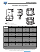
PRODUCT SUMMARY
V
DS
(V) R
DS(on)
(Ω)I
D
(A)
- 60
0.065 at V
GS
= - 10 V
- 5.7
0.110 at V
GS
= - 4.5 V
- 4.4
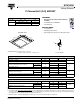
1
2
3
4
5
6
7
8
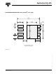
S
S
S
G
D
D
D
D
3.30 mm
3.30 mm
PowerPAK 1212-8
Bottom View
Ordering Information: Si7415DN-T1-E3 (Lead (Pb)-free)
Si7415DN-T1-GE3 (Lead (Pb)-free and Halogen-free)
S
G
D
P-Channel MOSFE
T
Notes:
a. Surface Mounted on 1" x 1" FR4 board.
b. See Solder Profile (www.vishay.com/ppg?73257
). The PowerPAK 1212-8 is a leadless package. The end of the lead terminal is exposed
copper (not plated) as a result of the singulation process in manufacturing. A solder fillet at the exposed copper tip cannot be guaranteed and
is not required to ensure adequate bottom side solder interconnection.
c. Rework Conditions: manual soldering with a soldering iron is not recommended for leadless components.
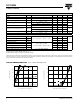
ABSOLUTE MAXIMUM RATINGS T
A
= 25 °C, unless otherwise noted
Parameter Symbol 10 s Steady State Unit
Drain-Source Voltage
V
DS
- 60
V
Gate-Source Voltage
V
GS
± 20
Continuous Drain Current (T
J
= 150 °C)
a
T
A
= 25 °C
I
D
- 5.7 - 3.6
A
T
A
= 70 °C
- 4.6 - 2.9
Pulsed Drain Current
I
DM
- 30
Continuous Source Current (Diode Conduction)
a
I
S
- 3.2 - 1.3
Maximum Power Dissipation
a
T
A
= 25 °C
P
D
3.8 1.5
W
T
A
= 70 °C
2.0 0.8
Operating Junction and Storage Temperature Range
T
J
, T
stg
- 55 to 150
°C
Soldering Recommendations (Peak Temperature)
b, c
260
THERMAL RESISTANCE RATINGS
Parameter Symbol Typical Maximum Unit
Maximum Junction-to-Ambient
a
t ≤ 10 s
R
thJA
26 33
°C/W
Steady State 65 81
Maximum Junction-to-Case (Drain) Steady State
R
thJC
1.9 2.4