
Datasheet


SiHA22N60EF
www.vishay.com
Vishay Siliconix
S19-0120-Rev. A, 04-Feb-2019
4
Document Number: 92250
For technical questions, contact: hvm@vishay.com
THIS DOCUMENT IS SUBJECT TO CHANGE WITHOUT NOTICE. THE PRODUCTS DESCRIBED HEREIN AND THIS DOCUMENT
ARE SUBJECT TO SPECIFIC DISCLAIMERS, SET FORTH AT www.vishay.com/doc?91000
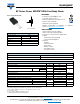
Fig. 7 - Typical Gate Charge vs. Gate-to-Source Voltage
Fig. 8 - Typical Source-Drain Diode Forward Voltage
Fig. 9 - Maximum Safe Operating Area
Note
a. V
GS
> minimum V
GS
at which R
DS(on)
is specified
Fig. 10 - Maximum Drain Current vs. Case Temperature
Fig. 11 - Temperature vs. Drain-to-Source Voltage
10
100
1000
10000
0
3
6
9
12
0 15304560
Axis Title
1st line
2nd line
2nd line
V
GS
- Gate-to-Source Voltage (V)
Q
g
- Total Gate Charge (nC)
V
DS
= 480 V
V
DS
= 300 V
V
DS
= 120 V
10
100
1000
10000
0.1
1
10
100
0.2 0.4 0.6 0.8 1.0 1.2 1.4
Axis Title
1st line
2nd line
2nd line
I
SD
- Reverse Drain Current (A)
V
SD
- Source-Drain Voltage (V)
T
J
= 25 °C
T
J
= 150 °C
V
GS
= 0 V
10
100
1000
10000
0.01
0.1
1
10
100
1101001000
Axis Title
1st line
2nd line
2nd line
I
D
- Drain Current (A)
V
DS
- Drain-to-Source Voltage (V)
I
DM
limited
T
C
= 25 °C,
T
J
= 150 °C,
single pulse
Limited by R
DS(on)
a
BVDSS limited
10 ms
1 ms
100 µs
Operation in this area
limited by R
DS(on)
10
100
1000
10000
0
5
10
15
20
25 50 75 100 125 150
Axis Title
1st line
2nd line
2nd line
I
D
- Drain Current (A)
T
C
- Case Temperature (°C)
10
100
1000
10000
600
625
650
675
700
725
750
775
-60 -40 -20 0 20 40 60 80 100 120 140 160
Axis Title
1st line
2nd line
2nd line
V
DS
- Drain-to-Source Breakdown Voltage (V)
T
J
- Junction Temperature (°C)
I
D
= 1 mA