
Datasheet


TEMT7000X01
www.vishay.com
Vishay Semiconductors
Rev. 1.2, 18-Oct-11
3
Document Number: 81961
For technical questions, contact: detectortechsupport@vishay.com
THIS DOCUMENT IS SUBJECT TO CHANGE WITHOUT NOTICE. THE PRODUCTS DESCRIBED HEREIN AND THIS DOCUMENT
ARE SUBJECT TO SPECIFIC DISCLAIMERS, SET FORTH AT www.vishay.com/doc?91000
Fig. 4 - Rise/Fall Time vs. Collector Current
Fig. 5 - Relative Spectral Sensitivity vs. Wavelength
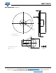
Fig. 6 - Relative Radiant Sensitivity vs. Angular Displacement
Fig. 7 - Relative Collector Current vs. Ambient Temperature
REFLOW SOLDER PROFILE
Fig. 8 - Lead (Pb)-free Reflow Solder Profile acc. J-STD-020
DRYPACK
Devices are packed in moisture barrier bags (MBB) to
prevent the products from moisture absorption during
transportation and storage. Each bag contains a desiccant.
FLOOR LIFE
Floor life (time between soldering and removing from MBB)
must not exceed the time indicated on MBB label:
Floor life: 168 h
Conditions: T
amb
< 30 °C, RH < 60 %
Moisture sensitivity level 3, acc. to J-STD-020.
DRYING
In case of moisture absorption devices should be baked
before soldering. Conditions see J-STD-020 or label.
Devices taped on reel dry using recommended conditions
192 h at 40 °C (+ 5 °C), RH < 5 %.
0
10
20
30
40
50
60
70
80
90
100
0 250 500 750 1000 1250 1500 1750 2000
I
C
- Collector Current (µA)
t
r
/t
f
- Rise/Fall Time (µs)
t
f
t
r
20599
R
L
= 100 Ω
0
0.2
0.4
0.6
0.8
1.0
1.2
400 500 600 700 800 900 1000 1100
21555
λ - Wavelength (nm)
S (λ)
rel
- Relative Spectral Sensitivity
0.4 0.2 0
I
e, rel
- Relative Radiant Sensitivity
94 8013
0.6
0.9
0.8
0°
30°
10° 20°
40°
50°
60°
70°
80°
0.7
1.0
ϕ - Angular Displacement
0
0.6
0.8
1.0
1.2
1.4
2.0
20 40 60 80
100
1.6
1.8
λ
94 8239
T
amb
- Ambient Temperature (°C)
I
ca rel
- Relative Collector Current
V
CE
= 5 V
E
e
= 1 mW/cm
2
= 950 nm
0
50
100
150
200
250
300
0 50 100 150 200 250 300
Time (s)
Temperature (°C)
240 °C
245 °C
max. 260 °C
max. 120 s
max. 100 s
217 °C
max. 30 s
max. ramp up 3 °C/s
max. ramp down 6 °C/s
19841
255 °C