
Datasheet


VLMR51Z1AA, VLMK51Z1AA, VLMY51Z1AA
www.vishay.com
Vishay Semiconductors
Rev. 1.4, 03-Sep-13
7
Document Number: 83419
For technical questions, contact: LED@vishay.com
THIS DOCUMENT IS SUBJECT TO CHANGE WITHOUT NOTICE. THE PRODUCTS DESCRIBED HEREIN AND THIS DOCUMENT
ARE SUBJECT TO SPECIFIC DISCLAIMERS, SET FORTH AT www.vishay.com/doc?91000
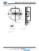
RECOMMENDED PAD DESIGN DIMENSIONS in millimeters
specications
according to DIN
technical drawings
Drawing-No.: 6.541-5084.01-4
Issue: 1 ; 13.04.10
22103
Recommended solder pad
Additional area covered by solder resist
for improved heat dissipation.
Package mark
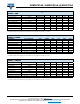
3.5 ± 0.2
3.5 ± 0.2
0.05
3.7 ± 0.2
Ø 2.6
1.5
3.1
0.5
0.7
1.2 ± 0.2
2.6
0.5
2.8
10
9.4
1.4
3.4
4.5
A
C