
Datasheet
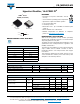

VS-16EDH02-M3
www.vishay.com
Vishay Semiconductors
Revision: 20-Mar-2019
1
Document Number: 95816
For technical questions within your region: DiodesAmericas@vishay.com
, DiodesAsia@vishay.com, DiodesEurope@vishay.com
THIS DOCUMENT IS SUBJECT TO CHANGE WITHOUT NOTICE. THE PRODUCTS DESCRIBED HEREIN AND THIS DOCUMENT
ARE SUBJECT TO SPECIFIC DISCLAIMERS, SET FORTH AT www.vishay.com/doc?91000
Hyperfast Rectifier, 16 A FRED Pt
®
DESIGN SUPPORT TOOLS AVAILABLE
FEATURES
• Hyperfast recovery time, reduced Q
rr
, and soft
recovery
• 175 °C maximum operating junction temperature
• Specified for output and snubber operation
• Low forward voltage drop
• Low leakage current
• Meets MSL level 1, per J-STD-020, LF maximum peak
of 260 °C
• Meets JESD 201 class 2 whisker test
• Material categorization: for definitions of compliance
please see www.vishay.com/doc?99912
DESCRIPTION / APPLICATIONS
State of the art hyperfast recovery rectifiers specifically
designed with optimized performance of forward voltage
drop and hyperfast recovery time.
The planar structure and the platinum doped life time control
guarantee the best overall performance, ruggedness, and
reliability characteristics.
These devices are intended for use in the output rectification
stage of SMPS, telecom, DC/DC converters as well as
freewheeling diode in low voltage inverters and chopper
motor drives.
Their extremely optimized stored charge and low recovery
current minimize the switching losses and reduce power
dissipation in the switching element.
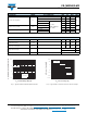
PRIMARY CHARACTERISTICS
I
F(AV)
16 A
V
R
200 V
V
F
at I
F
0.75 V
t
rr
32 ns
T
J
max. 175 °C
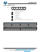
Package SMPD (TO-263AC)
Circuit configuration Single
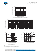
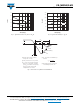
Top View Bottom View
Anode 1
Anode 2
K
Cathode
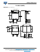
eSMP
®
Series
SMPD (TO-263AC)
K
1
2
3
3
D
D
3
D
3D Models
ABSOLUTE MAXIMUM RATINGS
PARAMETER SYMBOL TEST CONDITIONS VALUES UNITS
Peak repetitive reverse voltage V
RRM
200 V
Average rectified forward current I
F(AV)
T
solder pad
= 153 °C 16
A
Non-repetitive peak surge current I
FSM
T
J
= 25 °C, 6 ms square pulse 250
ELECTRICAL SPECIFICATIONS (T
J
= 25 °C unless otherwise specified)
PARAMETER SYMBOL TEST CONDITIONS MIN. TYP. MAX. UNITS
Breakdown voltage,
blocking voltage
V
BR
,
V
R
I
R
= 100 μA 200 - -
V
Forward voltage V
F
I
F
= 16 A - 0.91 1.0
I
F
= 16 A, T
J
= 150 °C - 0.75 0.84
Reverse leakage current I
R
V
R
= V
R
rated - - 15
μA
T
J
= 150 °C, V
R
= V
R
rated - 20 500
Junction capacitance C
T
V
R
= 200 V - 60 - pF