
User`s guide


SMPS AC/DC Reference Design User’s Guide
DS70320B-page 104 © 2008 Microchip Technology Inc.
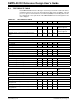
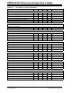
B.8 TEST RESULTS TABLE
Each SMPS AC/DC Reference Design is extensively tested from no/full load starts to
maximum current steps across the universal input voltage range. In addition, each unit
passes a rigorous 12-hour burn-in test at full load (300W). The following table shows
the complete list of tests performed on the SMPS AC/DC Reference Design before the
unit is shipped.
TABLE B-1: TEST RESULTS TABLE
Tests Min Max Units Result Remarks
Input Current
Max input current at 110 V
AC — 5 A 3.75 Loading VOUT2 @ 56A
and V
OUT3 @ 23A
Max input current at 220 VAC — 1.8 A 1.73 Loading VOUT2 @ 56A
and V
OUT3 @ 23A
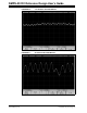
Maximum in-rush current at V
IN @ 220 VAC @ No
Load
—35 A 27
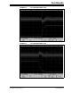
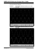
Output Overshoot at Start-up
V
IN = 110 VAC
VOUT1 @ 0A — 12.48 V 12
VOUT2 @ 0A — 3.432 V 3.3
V
OUT3 @ 0A — 5.2 V 5
VIN = 220 VAC
VOUT1 @ 0A — 12.48 V 12
V
OUT2 @ 0A — 3.432 V 3.3
VOUT3 @ 0A — 5.2 V 5
Power Factor
V
IN = 110 VAC @ No Load @ 60Hz 0.9 — — 0.974
VIN = 220 VAC @ No Load @ 50Hz 0.8 — — 0.855
V
IN = 110 VAC @ Full Load @ 60Hz 0.98 — — 0.997
VIN = 220 VAC @ Full Load @ 50Hz 0.97 — — 0.989
Input current THD @ VTHD @ 2%
Measured by power
meter
V
IN = 110 VAC @ Full Load @ 60Hz — 5 % 4.9
V
IN = 220 VAC @ Full Load @ 50Hz — 7 % 6
Input Power
V
OUT1 @ 30 A, VIN @ 110 VAC — — watt 445
V
OUT1 @ 0A, VOUT2 @ 56A, VOUT3 @ 23A,
V
IN @ 110 VAC
— — watt 415
V
OUT1 @ 30 A, VIN @ 220 VAC — — watt 431
VOUT1 @ 0A, VOUT2 @ 56A, VOUT3 @ 23A,
V
IN @ 220 VAC
— —watt400