
User`s guide


SMPS AC/DC REFERENCE
DESIGN USER’S GUIDE
© 2008 Microchip Technology Inc. DS70320B-page 51
Chapter 3. Software Design
3.1 OVERVIEW
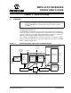
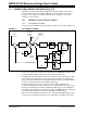
The SMPS AC/DC Reference Design is controlled using two dsPIC DSCs as shown in
the block diagram in Figure 3-1.
The dsPIC DSC on the primary side (on the left of the isolation barrier in Figure 3-1)
controls the PFC Boost Converter and the Phase-Shift ZVT Converter. The dsPIC DSC
on the secondary side (on the right of the isolation barrier in Figure 3-1) controls the
Multi-Phase Buck Converter and the Single-Phase Buck Converter.
The secondary side dsPIC DSC also performs the function of measuring the output
voltage of the Phase-Shift ZVT Converter, and feeding back to the primary side dsPIC
DSC as a digital feedback signal.
FIGURE 3-1: BLOCK DIAGRAM OF SMPS AC/DC REFERENCE DESIGN
Note: Any libraries and source files associated with SMPS AC/DC Reference
Design are available by request from your local Microchip sales office. See
the Microchip Web site, or the last page of this document for contact
information.
85-265 VAC
45-65 Hz
EMI Filter
and Bridge
Rectifier
PFC
Boost
Converter
ZVT
Full-Bridge
Converter
Synchronous
Rectifier
Opto-
Coupler
3.3 V
DC
69A
5 V
DC
23A
Isolation
Barrier
420 V
DC
Rectified
Sinusoidal
Voltage
Multi-Phase
Buck Converter
Single-Phase
Buck Converter
Phase-Shift ZVT Converter
dsPIC33FJ16GS504
dsPIC33FJ16GS504
12 VDC
30A