
User`s guide


Software Design
© 2008 Microchip Technology Inc. DS70320B-page 55
3.3.1.1.1 Digital PFC Implementation Using the dsPIC DSC
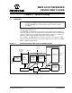
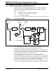
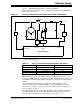
Figure 3-4 shows the hardware resources utilized on the primary side dsPIC DSC for
Power Factor Correction.
FIGURE 3-4: dsPIC
®
DSC RESOURCE ALLOCATION FOR PFC BOOST CONVERTER
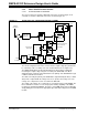
Table 3-1 lists the resources used on the dsPIC DSC for implementing the PFC control
scheme shown in Figure 3-3.
TABLE 3-1: dsPIC
®
DSC RESOURCES FOR PFC BOOST CONVERTER
The control of the PFC Boost Converter is obtained by varying the duty cycle of the
PWM signal. Only one pin of the PWM is utilized for the PFC control scheme, and
therefore the PWM module is configured for independent output mode. The frequency
of the PWM is determined by the hardware design. It is configured to be approximately
125 kHz.
The Analog Inputs AN4 and AN5 are configured to sample simultaneously. A
conversion is triggered on both AN4 and AN5 once every 3 PWM cycles, and the
current loop is executed on every conversion. The voltage loop is executed only once
in 15 current loop executions.
The Analog Input AN3 measures the AC Input voltage, which is used for generating a
sinusoidal current reference. In the SMPS AC/DC Reference Design, the current
reference value is calculated when the current loop is executed.
VAC
IPFC
VHV_BUS
ADC Channel
ADC
Channel
ADC
Channel
PWM
Output
|V
AC|
k
1
k
2
k
3
FET Driver
dsPIC33FJ16GS504
Description Type of Signal dsPIC
®
DSC Resource Used
V
HV_BUS Analog Input AN5
PFC Current (I
PFC) Analog Input AN4
|VAC| Sense Analog Input AN3
MOSFET Gate Drive Drive Output PWM4L