
User`s guide


SMPS AC/DC Reference Design User’s Guide
DS70320B-page 56 © 2008 Microchip Technology Inc.
3.3.2 Phase-Shift ZVT Control Scheme
3.3.2.1 ZVT RESOURCE ALLOCATION
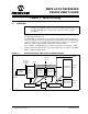
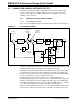
The control scheme for the Phase-Shift ZVT Converter is shown in Figure 3-5. A
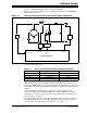
schematic of the Phase-Shift ZVT Converter is shown in Figure 3-6.
FIGURE 3-5: PHASE-SHIFT ZVT CONVERTER CONTROL SCHEME
The ZVT converter uses voltage mode control to maintain a constant output voltage.
The circuit configuration of the ZVT converter has the output voltage (the parameter to
be controlled) on the secondary side of the isolation barrier (refer to Figure 3-8).
The SMPS AC/DC Reference Design implements the ZVT voltage feedback by
measuring the output voltage using the secondary side dsPIC DSC. The Most
Significant 8 bits of data are transmitted back to the primary side dsPIC DSC through
a UART communication channel.
The data received by the primary side dsPIC DSC is right-shifted by two bits (for 10-bit
data) and is compared with the voltage reference to produce the voltage error. The
voltage error compensator is then executed in the ADC ISR.
The output of the voltage error compensator is feed into the phase-shifted PWM. The
Phase-Shift ZVT converter uses the unique phase-shifting capability of the PWM
module in the dsPIC33FJ16GS504. The phase of the PWM signal can be modified by
simply writing the new value in the appropriate Special Function Register in the PWM
module.
Σ
+
-
Voltage
Reference
VOUT
ZVT
Transformer
Voltage
Update
Phase
Overcurrent
Protection
ZVT Current Sense
V
OUT
Sense
Voltage Error
Compensator
ADC
1001011011
1011001010
S&H
S&H
Rectifier
Optocoupler
S&H
for overcurrent
protection
ADC
1011001010
UART
TX
UART
RX
Feedback
PWM