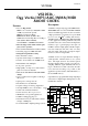
VS1053 B VS1053b VS1053b Ogg Vorbis/MP3/AAC/WMA/MIDI AUDIO CODEC Features Description • Decodes Ogg Vorbis; VS1053b is a single-chip Ogg Vorbis/MP3/AAC/MPEG 1 & 2 audio layer III (CBR +VBR WMA/MIDI audio decoder and an IMA ADPCM +ABR); layers I & II optional; and user-loadable Ogg Vorbis encoder. It contains MPEG4 / 2 AAC-LC(+PNS), a high-performance, proprietary low-power DSP HE-AAC v2 (Level 3) (SBR + PS); processor core VS DSP4 , working data memory, WMA 4.0/4.
VLSI VS1053b y Solution VS1053 B CONTENTS Contents 1 Licenses 9 2 Disclaimer 9 3 Definitions 9 4 Characteristics & Specifications 10 4.1 Absolute Maximum Ratings . . . . . . . . . . . . . . . . . . . . . . . . . . . . . . . . 10 4.2 Recommended Operating Conditions . . . . . . . . . . . . . . . . . . . . . . . . . . . . 10 4.3 Analog Characteristics . . . . . . . . . . . . . . . . . . . . . . . . . . . . . . . . . . . 11 4.4 Power Consumption . . . . . . . . . . . . . . . . . . .
VLSI VS1053b y Solution 7.4 CONTENTS Serial Protocol for Serial Data Interface (SDI) . . . . . . . . . . . . . . . . . . . . . . . 19 7.4.1 General . . . . . . . . . . . . . . . . . . . . . . . . . . . . . . . . . . . . . . . 19 7.4.2 SDI in VS1002 Native Modes (New Mode) . . . . . . . . . . . . . . . . . . . . 19 7.4.3 SDI in VS1001 Compatibility Mode (deprecated) . . . . . . . . . . . . . . . . . 20 7.4.4 Passive SDI Mode . . . . . . . . . . . . . . . . . . . . . . . . . . . . . . . . .
VLSI VS1053b y Solution 9 VS1053 B CONTENTS 8.2.7 Supported RIFF WAV Formats . . . . . . . . . . . . . . . . . . . . . . . . . . . 31 8.2.8 Supported MIDI Formats . . . . . . . . . . . . . . . . . . . . . . . . . . . . . . 32 8.3 Data Flow of VS1053b . . . . . . . . . . . . . . . . . . . . . . . . . . . . . . . . . . . 34 8.4 EarSpeaker Spatial Processing . . . . . . . . . . . . . . . . . . . . . . . . . . . . . . . 35 8.5 Serial Data Interface (SDI) . . . . . . . . . . . . . . . . . . .
VLSI Solution VS1053b y 9.5 VS1053 B CONTENTS Play and Decode . . . . . . . . . . . . . . . . . . . . . . . . . . . . . . . . . . . . . . 49 9.5.1 Playing a Whole File . . . . . . . . . . . . . . . . . . . . . . . . . . . . . . . . 49 9.5.2 Cancelling Playback . . . . . . . . . . . . . . . . . . . . . . . . . . . . . . . . 50 9.5.3 Fast Play . . . . . . . . . . . . . . . . . . . . . . . . . . . . . . . . . . . . . . 50 9.5.4 Fast Forward and Rewind without Audio . . . . . . . . . . . . . .
VLSI Solution VS1053b y VS1053 B CONTENTS 9.12.2 Pin Test . . . . . . . . . . . . . . . . . . . . . . . . . . . . . . . . . . . . . . . 63 9.12.3 SCI Test . . . . . . . . . . . . . . . . . . . . . . . . . . . . . . . . . . . . . . . 64 9.12.4 Memory Test . . . . . . . . . . . . . . . . . . . . . . . . . . . . . . . . . . . . 64 9.12.5 New Sine and Sweep Tests . . . . . . . . . . . . . . . . . . . . . . . . . . . . . 64 10 VS1053b Registers 66 10.1 Who Needs to Read This Chapter . . . . . . . .
VLSI Solution VS1053b y VS1053 B CONTENTS 10.11.2 Configuration TIMER CONFIG . . . . . . . . . . . . . . . . . . . . . . . . . . 73 10.11.3 Configuration TIMER ENABLE . . . . . . . . . . . . . . . . . . . . . . . . . . 74 10.11.4 Timer X Startvalue TIMER Tx[L/H] . . . . . . . . . . . . . . . . . . . . . . . 74 10.11.5 Timer X Counter TIMER TxCNT[L/H] . . . . . . . . . . . . . . . . . . . . . . 74 10.11.6 Interrupts . . . . . . . . . . . . . . . . . . . . . . . . . . . . . . . . . . . . . .
VLSI Solution VS1053b y VS1053 B LIST OF FIGURES List of Figures 1 Pin Configuration, LQFP-48. . . . . . . . . . . . . . . . . . . . . . . . . . . . . . . . . 13 2 VS1053b in LQFP-48 Packaging. . . . . . . . . . . . . . . . . . . . . . . . . . . . . . 13 3 Typical Connection Diagram Using LQFP-48. . . . . . . . . . . . . . . . . . . . . . . . 16 4 BSYNC Signal - one byte transfer. . . . . . . . . . . . . . . . . . . . . . . . . . . . . . 20 5 BSYNC Signal - two byte transfer. . . . . . . .
VLSI VS1053b y Solution 1 VS1053 B 1. LICENSES Licenses MPEG Layer-3 audio decoding technology licensed from Fraunhofer IIS and Thomson. Note: If you enable Layer I and Layer II decoding, you are liable for any patent issues that may arise from using these formats. Joint licensing of MPEG 1.0 / 2.0 Layer III does not cover all patents pertaining to layers I and II. VS1053b contains WMA decoding technology from Microsoft.
VS1053 B VLSI VS1053b4. CHARACTERISTICS & SPECIFICATIONS y Solution 4 Characteristics & Specifications 4.1 Absolute Maximum Ratings Parameter Analog Positive Supply Digital Positive Supply I/O Positive Supply Current at Any Non-Power Pin1 Voltage at Any Digital Input Operating Temperature Storage Temperature 1 2 Symbol AVDD CVDD IOVDD Min -0.3 -0.3 -0.3 -0.3 -30 -65 Max 3.6 1.85 3.6 ±50 IOVDD+0.32 +85 +150 Unit V V V mA V ◦C ◦C Higher current can cause latch-up. Must not exceed 3.6 V 4.
VS1053 B VLSI VS1053b4. CHARACTERISTICS & SPECIFICATIONS y Solution 4.3 Analog Characteristics Unless otherwise noted: AVDD=3.3V, CVDD=1.8V, IOVDD=2.8V, REF=1.65V, TA=-30..+85◦ C, XTALI=12..13MHz, Internal Clock Multiplier 3.5×. DAC tested with 1307.894 Hz full-scale output sinewave, measurement bandwidth 20..20000 Hz, analog output load: LEFT to GBUF 30 Ω, RIGHT to GBUF 30 Ω. Microphone test amplitude 48 mVpp, fs =1 kHz, Line input test amplitude 1.26 V, fs =1 kHz.
VS1053 B VLSI VS1053b4. CHARACTERISTICS & SPECIFICATIONS y Solution 4.4 Power Consumption Tested with an MPEG 1.0 Layer-3 128 kbps sample and generated sine. Output at full volume. Internal clock multiplier 3.0×. TA=+25◦ C. Parameter Power Supply Consumption AVDD, Reset Power Supply Consumption CVDD = 1.8V, Reset Power Supply Consumption AVDD, sine test, 30 Ω + GBUF Power Supply Consumption CVDD = 1.
VLSI VS1053b y Solution 5 VS1053 B 5. PACKAGES AND PIN DESCRIPTIONS Packages and Pin Descriptions 5.1 Packages LPQFP-48 is a lead (Pb) free and also RoHS compliant package. RoHS is a short name of Directive 2002/95/EC on the restriction of the use of certain hazardous substances in electrical and electronic equipment. 5.1.1 LQFP-48 48 1 Figure 1: Pin Configuration, LQFP-48. LQFP-48 package dimensions are at http://www.vlsi.fi/ . Figure 2: VS1053b in LQFP-48 Packaging. Version 1.
VLSI VS1053b y Solution Pad Name MICP / LINE1 MICN XRESET DGND0 CVDD0 IOVDD0 CVDD1 DREQ GPIO2 / DCLK1 GPIO3 / SDATA1 GPIO6 / I2S SCLK3 GPIO7 / I2S SDATA3 XDCS / BSYNC1 IOVDD1 VCO DGND1 XTALO XTALI IOVDD2 DGND2 DGND3 DGND4 XCS CVDD2 GPIO5 / I2S MCLK3 RX TX SCLK SI SO CVDD3 XTEST GPIO0 GPIO1 GND GPIO4 / I2S LROUT3 AGND0 AVDD0 RIGHT AGND1 AGND2 GBUF AVDD1 RCAP AVDD2 LEFT AGND3 LINE2 LQFP Pin 1 2 3 4 5 6 7 8 9 10 11 12 13 14 15 16 17 18 19 20 21 22 23 24 25 26 27 28 29 30 31 32 33 34 35 36 37 38 39 40 41 4
VLSI Solution VS1053b y VS1053 B 5. PACKAGES AND PIN DESCRIPTIONS Pin types: Type DI DO DIO DO3 AI Version 1.
VLSI VS1053b y Solution 6 VS1053 B 6. CONNECTION DIAGRAM, LQFP-48 Connection Diagram, LQFP-48 Figure 3: Typical Connection Diagram Using LQFP-48. Figure 3 shows a typical connection diagram for VS1053. Figure Note 1: Connect either Microphone In or Line In, but not both at the same time. Note: This connection assumes SM SDINEW is active (see Chapter 8.7.1). If also SM SDISHARE is used, xDCS should be tied low or high (see Chapter 7.2.1). Version 1.
VLSI Solution VS1053b y VS1053 B 6. CONNECTION DIAGRAM, LQFP-48 The common buffer GBUF can be used for common voltage (1.23 V) for earphones. This will eliminate the need for large isolation capacitors on line outputs, and thus the audio output pins from VS1053b may be connected directly to the earphone connector. GBUF must NOT be connected to ground under any circumstances. If GBUF is not used, LEFT and RIGHT must be provided with coupling capacitors.
VLSI VS1053b y Solution 7 VS1053 B 7. SPI BUSES SPI Buses 7.1 General The SPI Bus - that was originally used in some Motorola devices - has been used for both VS1053b’s Serial Data Interface SDI (Chapters 7.4 and 8.5) and Serial Control Interface SCI (Chapters 7.5 and 8.6). 7.2 SPI Bus Pin Descriptions 7.2.1 VS1002 Native Modes (New Mode) These modes are active on VS1053b when SM SDINEW is set to 1 (default at startup).
VLSI VS1053b y Solution 7.3 VS1053 B 7. SPI BUSES Data Request Pin DREQ The DREQ pin/signal is used to signal if VS1053b’s 2048-byte FIFO is capable of receiving data. If DREQ is high, VS1053b can take at least 32 bytes of SDI data or one SCI command. DREQ is turned low when the stream buffer is too full and for the duration of a SCI command.
VLSI Solution VS1053b y 7.4.3 VS1053 B 7. SPI BUSES SDI in VS1001 Compatibility Mode (deprecated) BSYNC SDATA D7 D6 D5 D4 D3 D2 D1 D0 DCLK Figure 4: BSYNC Signal - one byte transfer. When VS1053b is running in VS1001 compatibility mode, a BSYNC signal must be generated to ensure correct bit-alignment of the input bitstream.
VLSI Solution VS1053b y 7.5.2 VS1053 B 7. SPI BUSES SCI Read XCS 0 1 2 3 4 5 6 7 8 9 10 11 12 13 14 15 16 17 0 0 0 0 0 0 1 1 0 0 0 30 31 SCK 3 SI instruction (read) 2 1 0 don’t care 0 data out address 15 14 SO 0 0 0 0 0 0 0 0 0 0 0 0 0 don’t care 0 0 1 0 0 X execution DREQ Figure 6: SCI Word Read VS1053b registers are read from using the following sequence, as shown in Figure 6. First, XCS line is pulled low to select the device.
VLSI VS1053b y Solution VS1053 B 7. SPI BUSES After the word has been shifted in and the last clock has been sent, XCS should be pulled high to end the WRITE sequence. After the last bit has been sent, DREQ is driven low for the duration of the register update, marked “execution” in the figure. The time varies depending on the register and its contents (see table in Chapter 8.7 for details).
VLSI VS1053b y Solution 7.6 VS1053 B 7. SPI BUSES SPI Timing Diagram tWL tXCSS tWH tXCSH XCS 0 1 14 15 30 16 31 tXCS SCK SI tH tSU SO tZ tV tDIS Figure 9: SPI Timing Diagram. Symbol tXCSS tSU tH tZ tWL tWH tV tXCSH tXCS tDIS 1 Min 5 0 2 0 2 2 2 (+ 25 ns1 ) 1 2 Max 10 Unit ns ns CLKI cycles ns CLKI cycles CLKI cycles CLKI cycles CLKI cycles CLKI cycles ns 25 ns is when pin loaded with 100 pF capacitance. The time is shorter with lower capacitance.
VLSI VS1053b y Solution 7.7 7.7.1 VS1053 B 7. SPI BUSES SPI Examples with SM SDINEW and SM SDISHARED set Two SCI Writes SCI Write 1 SCI Write 2 XCS 0 1 2 3 30 31 1 0 32 33 61 62 63 2 1 0 SCK SI 0 0 0 0 X 0 0 X DREQ up before finishing next SCI write DREQ Figure 10: Two SCI Operations. Figure 10 shows two consecutive SCI operations. Note that xCS must be raised to inactive state between the writes. Also DREQ must be respected as shown in the figure. 7.7.
VLSI Solution VS1053b y 7.7.3 VS1053 B 7. SPI BUSES SCI Operation in Middle of Two SDI Bytes SDI Byte SDI Byte SCI Operation XCS 0 1 7 8 9 39 40 41 7 6 46 47 1 0 SCK 7 SI 6 5 1 0 0 5 X 0 DREQ high before end of next transfer DREQ Figure 12: Two SDI Bytes Separated By an SCI Operation. Figure 12 shows how an SCI operation is embedded in between SDI operations. xCS edges are used to synchronize both SDI and SCI. Remember to respect DREQ as shown in the figure. Version 1.
VLSI VS1053b y Solution 8 VS1053 B 8. FUNCTIONAL DESCRIPTION Functional Description 8.1 Main Features VS1053b is based on a proprietary digital signal processor, VS DSP. It contains all the code and data memory needed for Ogg Vorbis, MP3, AAC, WMA and WAV PCM + ADPCM audio decoding, MIDI synthesizer, together with serial interfaces, a multirate stereo audio DAC and analog output amplifiers and filters.
VLSI Solution VS1053b y 8.2.2 VS1053 B 8. FUNCTIONAL DESCRIPTION Supported MP1 (MPEG layer I) Formats Note: Layer I / II decoding must be specifically enabled from register SCI MODE. MPEG 1.
VLSI Solution VS1053b y 8.2.5 VS1053 B 8. FUNCTIONAL DESCRIPTION Supported AAC (ISO/IEC 13818-7 and ISO/IEC 14496-3) Formats VS1053b decodes MPEG2-AAC-LC-2.0.0.0 and MPEG4-AAC-LC-2.0.0.0 streams, i.e. the low complexity profile with maximum of two channels can be decoded. If a stream contains more than one element and/or element type, you can select which one to decode from the 16 single-channel, 16 channelpair, and 16 low-frequency elements.
VLSI VS1053b y Solution VS1053 B 8. FUNCTIONAL DESCRIPTION AAC12 : Samplerate / Hz 48000 44100 32000 24000 22050 16000 12000 11025 8000 ≤96 + + + + + + + + + Maximum Bitrate kbit/s - for 2 channels 132 144 192 264 288 384 529 + + + + + + + + + + + + + + + + + + + + + + + + + + + + + + + + + + + 576 + 1 64000 Hz, 88200 Hz, and 96000 Hz AAC files are played at the highest possible samplerate (48000 Hz with 12.288 MHz XTALI). 2 Also all variable bitrate (VBR) formats are supported.
VLSI Solution VS1053b y 8.2.6 VS1053 B 8. FUNCTIONAL DESCRIPTION Supported WMA Formats Windows Media Audio codec versions 2, 7, 8, and 9 are supported. All WMA profiles (L1, L2, and L3) are supported. Previously streams were separated into Classes 1, 2a, 2b, and 3. The decoder has passed Microsoft’s conformance testing program. Windows Media Audio Professional is a different codec and is not supported. WMA 4.0 / 4.
VLSI Solution VS1053b y 8.2.7 VS1053 B 8. FUNCTIONAL DESCRIPTION Supported RIFF WAV Formats The most common RIFF WAV subformats are supported, with 1 or 2 audio channels. Format 0x01 0x02 0x03 0x06 0x07 0x10 0x11 0x15 0x16 0x30 0x31 0x3b 0x3c 0x40 0x41 0x50 0x55 0x64 0x65 Version 1.
VLSI Solution VS1053b y 8.2.8 VS1053 B 8. FUNCTIONAL DESCRIPTION Supported MIDI Formats General MIDI and SP-MIDI format 0 files are played. Format 1 and 2 files must be converted to format 0 by the user. The maximum polyphony is 64, the maximum sustained polyphony is 40.
VLSI Solution VS1053b y 1 Acoustic Grand Piano 2 Bright Acoustic Piano 3 Electric Grand Piano 4 Honky-tonk Piano 5 Electric Piano 1 6 Electric Piano 2 7 Harpsichord 8 Clavi 9 Celesta 10 Glockenspiel 11 Music Box 12 Vibraphone 13 Marimba 14 Xylophone 15 Tubular Bells 16 Dulcimer 17 Drawbar Organ 18 Percussive Organ 19 Rock Organ 20 Church Organ 21 Reed Organ 22 Accordion 23 Harmonica 24 Tango Accordion 25 Acoustic Guitar (nylon) 26 Acoustic Guitar (steel) 27 Electric Guitar (jazz) 28 Electric Guitar (clea
VLSI VS1053b y Solution 8.3 VS1053 B 8. FUNCTIONAL DESCRIPTION Data Flow of VS1053b SDI Bitstream FIFO MP3 MP2 MP1 WAV ADPCM WMA AAC MIDI Vorbis SM_ADPCM=0 AIADDR = 0 User Application AIADDR != 0 SB_AMPLITUDE=0 Bass enhancer Treble control SB_AMPLITUDE!=0 Audio FIFO 2048 stereo samples ST_AMPLITUDE=0 Ear Speaker ST_AMPLITUDE!=0 L S.rate.conv. R and DAC Volume SCI_VOL control Figure 13: Data Flow of VS1053b.
VLSI VS1053b y Solution 8.4 VS1053 B 8. FUNCTIONAL DESCRIPTION EarSpeaker Spatial Processing While listening to headphones the sound has a tendency to be localized inside the head. The sound field becomes flat and lacking the sensation of dimensions. This is an unnatural, awkward and sometimes even disturbing situation. This phenomenon is often referred in literature as ‘lateralization’, meaning ’in-the-head’ localization. Long-term listening to lateralized sound may lead to listening fatigue.
VLSI VS1053b y Solution 8.5 VS1053 B 8. FUNCTIONAL DESCRIPTION Serial Data Interface (SDI) The serial data interface is meant for transferring compressed data for the different decoders of VS1053b. If the input of the decoder is invalid or it is not received fast enough, analog outputs are automatically muted. Also several different tests may be activated through SDI as described in Chapter 9. 8.
VLSI VS1053b y Solution 8.7 VS1053 B 8. FUNCTIONAL DESCRIPTION SCI Registers VS1053b sets DREQ low when it detects an SCI operation (this delay is 16 to 40 CLKI cycles depending on whether an interrupt service routine is active) and restores it when it has processed the operation. The duration depends on the operation. If DREQ is low when an SCI operation is performed, it also stays low after SCI operation processing.
VLSI Solution VS1053b y 8.7.1 VS1053 B 8. FUNCTIONAL DESCRIPTION SCI MODE (RW) SCI MODE is used to control the operation of VS1053b and defaults to 0x0800 (SM SDINEW set).
VLSI Solution VS1053b y VS1053 B 8. FUNCTIONAL DESCRIPTION If SM TESTS is set, SDI tests are allowed. For more details on SDI tests, look at Chapter 9.12. SM STREAM activates VS1053b’s stream mode. In this mode, data should be sent with as even intervals as possible and preferable in blocks of less than 512 bytes, and VS1053b makes every attempt to keep its input buffer half full by changing its playback speed upto 5%. For best quality sound, the average speed error should be within 0.
VLSI VS1053b y Solution 8.7.2 VS1053 B 8. FUNCTIONAL DESCRIPTION SCI STATUS (RW) SCI STATUS contains information on the current status of VS1053b. It also controls some low-level things that the user does not usually have to care about. Name SS DO NOT JUMP SS SWING SS VCM OVERLOAD SS VCM DISABLE SS SS SS SS SS VER APDOWN2 APDOWN1 AD CLOCK REFERENCE SEL Bits 15 14:12 11 10 9:8 7:4 3 2 1 0 Description Header in decode, do not fast forward/rewind Set swing to +0 dB, +0.5 dB, .., or +3.
VLSI Solution VS1053b y 8.7.3 VS1053 B 8. FUNCTIONAL DESCRIPTION SCI BASS (RW) Name ST AMPLITUDE ST FREQLIMIT SB AMPLITUDE SB FREQLIMIT Bits 15:12 11:8 7:4 3:0 Description Treble Control in 1.5 dB steps (-8..7, 0 = off) Lower limit frequency in 1000 Hz steps (1..15) Bass Enhancement in 1 dB steps (0..15, 0 = off) Lower limit frequency in 10 Hz steps (2..
VLSI Solution VS1053b y 8.7.4 VS1053 B 8. FUNCTIONAL DESCRIPTION SCI CLOCKF (RW) The operation of SCI CLOCKF has changed slightly in VS1053b compared to VS1003 and VS1033. Multiplier 1.5× and addition 0.5× have been removed to allow higher clocks to be configured. Name SC MULT SC ADD SC FREQ SCI CLOCKF bits Bits Description 15:13 Clock multiplier 12:11 Allowed multiplier addition 10: 0 Clock frequency SC MULT activates the built-in clock multiplier. This will multiply XTALI to create a higher CLKI.
VLSI Solution VS1053b y 8.7.5 VS1053 B 8. FUNCTIONAL DESCRIPTION SCI DECODE TIME (RW) When decoding correct data, current decoded time is shown in this register in full seconds. The user may change the value of this register. In that case the new value should be written twice to make absolutely certain that the change is not overwritten by the firmware. A write to SCI DECODE TIME also resets the byteRate calculation. SCI DECODE TIME is reset at every hardware and software reset.
VLSI Solution VS1053b y SM WRAMADDR Start. . . End 0x1800. . . 0x18XX 0x5800. . . 0x58XX 0x8040. . . 0x84FF 0xC000. . . 0xFFFF Dest. addr. Start. . . End 0x1800. . . 0x18XX 0x1800. . . 0x18XX 0x0040. . . 0x04FF 0xC000. . . 0xFFFF Bits/ Word 16 16 32 16 VS1053 B 8. FUNCTIONAL DESCRIPTION Description X data RAM Y data RAM Instruction RAM I/O Only user areas in X, Y, and instruction memory are listed above. Other areas can be accessed, but should not be written to unless otherwise specified.
VLSI Solution VS1053b y 8.7.9 VS1053 B 8. FUNCTIONAL DESCRIPTION SCI HDAT0 and SCI HDAT1 (R) For WAV files, SCI HDAT1 contains 0x7665 (“ve”). SCI HDAT0 contains the data rate measured in bytes per second for all supported RIFF WAVE formats: mono and stereo 8-bit or 16-bit PCM, mono and stereo IMA ADPCM. To get the bitrate of the file, multiply the value by 8. For AAC ADTS streams, SCI HDAT1 contains 0x4154 (“AT”). For AAC ADIF files, SCI HDAT1 contains 0x4144 (“AD”). For AAC .mp4 / .
VLSI Solution VS1053 B VS1053b y 8. FUNCTIONAL DESCRIPTION When read, SCI HDAT0 and SCI HDAT1 contain header information that is extracted from MP3 stream currently being decoded. After reset both registers are cleared, indicating no data has been found yet.
VLSI Solution VS1053b y 8.7.11 VS1053 B 8. FUNCTIONAL DESCRIPTION SCI VOL (RW) SCI VOL is a volume control for the player hardware. The most significant byte of the volume register controls the left channel volume, the low part controls the right channel volume. The channel volume sets the attenuation from the maximum volume level in 0.5 dB steps. Thus, maximum volume is 0x0000 and total silence is 0xFEFE. Note, that after hardware reset the volume is set to full volume.
VLSI VS1053b y Solution 9 VS1053 B 9. OPERATION Operation 9.1 Clocking VS1053b operates on a single, nominally 12.288 MHz fundamental frequency master clock. This clock can be generated by external circuitry (connected to pin XTALI) or by the internal clock crystal interface (pins XTALI and XTALO). This clock is used by the analog parts and determines the highest available samplerate. With 12.288 MHz clock all samplerates upto 48000 Hz are available. VS1053b can also use 24..
VLSI VS1053b y Solution 9.4 VS1053 B 9. OPERATION Low Power Mode If you need to keep the system running while not decoding data, but need to lower the power consumption, you can use the following tricks. • Select the 1.0× clock by writing 0x0000 to SCI CLOCKF. This disables the PLL and saves some power. • Write a low non-zero value, such as 0x0010 to SCI AUDATA. This will reduce the samplerate and the number of audio interrupts required.
VLSI Solution VS1053b y 9.5.2 VS1053 B 9. OPERATION Cancelling Playback Cancelling playback of a song is a normal operation when the user wants to jump to another song while doing playback. 1. Send a portion of an audio file to VS1053b. 2. Set SCI MODE bit SM CANCEL. 3. Continue sending audio file, but check SM CANCEL after every 32 bytes of data. If it is still set, goto 3. If SM CANCEL doesn’t clear after 2048 bytes or one second, do a software reset (this should be extremely rare). 4.
VLSI Solution VS1053b y VS1053 B 9. OPERATION Note: It is recommended that playback volume is decreased by e.g. 10 dB when fast forwarding/rewinding. Note: Register DECODE TIME does not take jumps into account. Note: Midi is not suitable for random-access. You can implement fast forward using the playSpeed extra parameter to select 1-128× play speed. SCI DECODE TIME also speeds up. If necessary, rewind can be implemented by restarting decoding of a MIDI file and fast playing to the appropriate place.
VLSI VS1053b y Solution 9.6 VS1053 B 9. OPERATION Feeding PCM data VS1053b can be used as a PCM decoder by sending a WAV file header. If the length sent in the WAV header is 0xFFFFFFFF, VS1053b will stay in PCM mode indefinitely (or until SM CANCEL has been set). 8-bit linear and 16-bit linear audio is supported in mono or stereo.
VLSI VS1053b y Solution 9.8 VS1053 B 9. OPERATION ADPCM Recording This chapter explains how to create RIFF/WAV file with IMA ADPCM format. This is a widely supported ADPCM format and many PC audio playback programs can play it. IMA ADPCM recording gives roughly a compression ratio of 4:1 compared to linear, 16-bit audio. This makes it possible to record for example ono 8 kHz audio at 32.44 kbit/s.
VLSI Solution VS1053b y VS1053 B 9. OPERATION WriteVS10xxPatch() should perform the following SCI writes (only for VS1053b): Register SCI WRAMADDR SCI WRAM SCI WRAM SCI WRAM SCI WRAM SCI WRAM SCI WRAM SCI WRAM SCI WRAM SCI WRAM SCI WRAM SCI WRAM SCI WRAM SCI WRAM SCI WRAM SCI WRAM SCI WRAM SCI WRAM SCI WRAM SCI WRAM SCI WRAM SCI WRAM SCI WRAM SCI WRAM SCI WRAM SCI WRAM SCI WRAM SCI WRAM SCI WRAM SCI WRAMADDR SCI WRAM SCI WRAM Reg.
VLSI Solution VS1053b y 9.8.3 VS1053 B 9. OPERATION Adding a RIFF Header To make your IMA ADPCM file a RIFF / WAV file, you have to add a header before the actual data. The following shows a header for mono file.
VLSI Solution VS1053b y 9.8.4 VS1053 B 9. OPERATION Playing ADPCM Data In order to play back your IMA ADPCM recordings, you have to have a file with a header as described in Chapter 9.8.3. If this is the case, all you need to do is to provide the ADPCM file through SDI as you would with any audio file. 9.8.5 Sample Rate Considerations VS10xx chips that support IMA ADPCM playback are capable of playing back ADPCM files with any sample rate.
VLSI VS1053b y Solution 9.9 VS1053 B 9. OPERATION SPI Boot If GPIO0 is set with a pull-up resistor to 1 at boot time, VS1053b tries to boot from external SPI memory. SPI boot redefines the following pins: Normal Mode GPIO0 GPIO1 DREQ GPIO2 SPI Boot Mode xCS CLK MOSI MISO The memory has to be an SPI Bus Serial EEPROM with 16-bit or 24-bit addresses. The serial speed used by VS1053b is 245 kHz with the nominal 12.288 MHz clock. The first three bytes in the memory have to be 0x50, 0x26, 0x48. 9.
VLSI Solution VS1053b y 9.11 VS1053 B 9. OPERATION Extra Parameters The following structure is in X memory at address 0x1e00 (note the different location than in VS1033) and can be used to change some extra parameters or get useful information. The chip ID is also easily available.
VLSI Solution VS1053b y VS1053 B 9. OPERATION You can see that in the invalid read the low part wraps from 0x0000 to 0xffff while the high part stays the same. In this case the second read gives a valid answer, otherwise always use the value of the first read. The second read is needed when it is possible that the low part wraps around, changing the high part, i.e. when the low part is small. bytesLeft is only decreased by one at a time, so a reread is needed only if the low part is 0. 9.11.
VLSI Solution VS1053b y VS1053 B 9. OPERATION positionMsec is a field that gives the current play position in a file in milliseconds, regardless of rewind and fast forward operations. The value is only available in codecs that can determine the play position from the stream itself. Currently WMA and Ogg Vorbis provide this information. If the position is unknown, this field contains -1. resync field is used to force a resynchronization to the stream for WMA and AAC (ADIF, .mp4 / .
VLSI VS1053b y Solution 9.11.3 VS1053 B 9. OPERATION AAC Parameter config1 sceFoundMask cpeFoundMask lfeFoundMask playSelect dynCompress dynBoost sbrAndPsStatus Address 0x1e03(7:4) 0x1e2a 0x1e2b 0x1e2c 0x1e2d 0x1e2e 0x1e2f 0x1e30 Usage SBR and PS select Single channel elements found Channel pair elements found Low frequency elements found Play element selection Compress coefficient for DRC, -8192=1.0 Boost coefficient for DRC, 8192=1.
VLSI Solution VS1053b y config1(7:6) ’00’ ’01’ ’10’ ’11’ VS1053 B 9. OPERATION Usage normal mode, process PS if it is available process PS if it is available, but in downsampled mode reserved disable PS processing AAC decoder can also increase the internal clock automatically when it detects that a file can not be decoded correctly with the current clock. The maximum allowed clock is configured with the SCI CLOCKF register.
VLSI Solution VS1053b y Gain -11 (-5.5 dB) -11 (-5.5 dB) +2 (+1.0 dB) +2 (+1.0 dB) +2 (+1.0 dB) 9.12 VS1053 B Volume 0 (+0.0 dB) 3 (-1.5 dB) 0 (+0.0 dB) 1 (-0.5 dB) 4 (-2.0 dB) 9. OPERATION SCI VOL (Volume-Gain) 0x0b0b (-5.5 dB) 0x0e0e (-7.0 dB) 0x0000 (+0.0 dB) 0x0000 (+0.0 dB) 0x0202 (-1.0 dB) SDI Tests There are several test modes in VS1053b, which allow the user to perform memory tests, SCI bus tests, and several different sine wave tests.
VLSI Solution VS1053b y 9.12.3 VS1053 B 9. OPERATION SCI Test Sci test is initialized with the 8-byte sequence 0x53 0x70 0xEE n 0 0 0 0, where n − 48 is the register number to test. The content of the given register is read and copied to SCI HDAT0. If the register to be tested is HDAT0, the result is copied to SCI HDAT1. Example: if n is 48, contents of SCI register 0 (SCI MODE) is copied to SCI HDAT0. 9.12.
VLSI Solution VS1053b y VS1053 B 9. OPERATION LSb’s of the SCI AICTRLn should be zero. The resulting frequencies Fsin can be calculated from the DAC samplerate Fs and SCI AICTRL0 / SCI AICTRL1 using the following equation. Fsin = SCI AICT RLn × F s /65536 Sine sweep test can be started by writing 0x4022 to SCI AIADDR. Both these tests use the normal audio path, thus also SCI BASS, differential output mode, and EarSpeaker settings have an effect. Version 1.
VLSI VS1053b y Solution 10 10.1 VS1053 B 10. VS1053B REGISTERS VS1053b Registers Who Needs to Read This Chapter User software is required when a user wishes to add some own functionality like DSP effects to VS1053b. However, most users of VS1053b don’t need to worry about writing their own code, or about this chapter, including those who only download software plug-ins from VLSI Solution’s Web site. 10.
VLSI Solution VS1053b y 10.5 10. VS1053B REGISTERS Serial Data Registers Reg 0xC011 0xC012 10.
VLSI Solution VS1053b y 10.8 VS1053 B 10. VS1053B REGISTERS Interrupt Registers Reg 0xC01A 0xC01B 0xC01C 0xC01D Type rw w w rw Reset 0 0 0 0 Interrupt registers, prefix INT Abbrev[bits] Description ENABLE[7:0] Interrupt enable GLOB DIS[-] Write to add to interrupt counter GLOB ENA[-] Write to subtract from interrupt counter COUNTER[4:0] Interrupt counter INT ENABLE controls the interrupts.
VLSI Solution VS1053b y 10.9 VS1053 B 10. VS1053B REGISTERS Watchdog v1.0 2002-08-26 The watchdog consist of a watchdog counter and some logic. After reset, the watchdog is inactive. The counter reload value can be set by writing to WDOG CONFIG. The watchdog is activated by writing 0x4ea9 to register WDOG RESET. Every time this is done, the watchdog counter is reset. Every 65536’th clock cycle the counter is decremented by one.
VLSI Solution VS1053 B VS1053b y 10.10 10. VS1053B REGISTERS UART v1.1 2004-10-09 RS232 UART implements a serial interface using rs232 standard. Start bit D0 D1 D2 D3 D4 D5 D6 Stop D7 bit Figure 15: RS232 Serial Interface Protocol When the line is idling, it stays in logic high state. When a byte is transmitted, the transmission begins with a start bit (logic zero) and continues with data bits (LSB first) and ends up with a stop bit (logic high). 10 bits are sent for each 8-bit byte frame.
VLSI Solution VS1053b y VS1053 B 10. VS1053B REGISTERS 10.10.3 Data UARTx DATA A read from UARTx DATA returns the received byte in bits 7:0, bits 15:8 are returned as ’0’. If there is no more data to be read, the receiver data register full indicator will be cleared. A receive interrupt will be generated when a byte is moved from the receiver shift register to the receiver data register. A write to UARTx DATA sets a byte for transmission.
VLSI Solution VS1053b y VS1053 B 10. VS1053B REGISTERS 10.10.6 Interrupts and Operation Transmitter operates as follows: After an 8-bit word is written to the transmit data register it will be transmitted instantly if the transmitter is not busy transmitting the previous byte. When the transmission begins a TX INTR interrupt will be sent. Status bit [1] informs the transmitter data register empty (or full state) and bit [0] informs the transmitter (shift register) empty state.
VLSI Solution VS1053b y 10.11 VS1053 B 10. VS1053B REGISTERS Timers v1.0 2002-04-23 There are two 32-bit timers that can be initialized and enabled independently of each other. If enabled, a timer initializes to its start value, written by a processor, and starts decrementing every clock cycle. When the value goes past zero, an interrupt is sent, and the timer initializes to the value in its start value register, and continues downcounting. A timer stays in that loop as long as it is enabled.
VLSI Solution VS1053b y VS1053 B 10. VS1053B REGISTERS 10.11.3 Configuration TIMER ENABLE Name TIMER EN T1 TIMER EN T0 TIMER ENABLE Bits Bits Description 1 Enable timer 1 0 Enable timer 0 10.11.4 Timer X Startvalue TIMER Tx[L/H] The 32-bit start value TIMER Tx[L/H] sets the initial counter value when the timer is reset. The timer fi interrupt frequency ft = c+1 where fi is the master clock obtained with the clock divider (see Chapter 10.11.2 and c is TIMER Tx[L/H].
VLSI Solution VS1053b y 10.12 VS1053 B 10. VS1053B REGISTERS VS1053b Audio Path MICN MICP LINE1 MIC AMP ADC MUX Stereo ADC LINE2 Audio FIFO Sample-Rate Converter Sigma-Delta Modulator + Analog Drivers LEFT RIGHT CBUF Volume Control SRC I2S SDM Figure 16: VS1053b ADC and DAC data paths In IMA ADPCM encoding mode the data from Analog-to-Digital conversion is first processed in 48 kHz or 24 kHz samplerate.
VLSI Solution VS1053b y 10.13 VS1053 B 10. VS1053B REGISTERS I2S DAC Interface The I2S Interface makes it possible to attach an external DAC to the system. Note: in VS1053b the I2S pins share different GPIO pins than in VS1033 to be able to use SPI boot and I2S in the same application. 10.13.1 Registers Reg 0xC040 I2S registers, prefix I2S Type Reset Abbrev Description r/w 0 CONFIG[3:0] I2S configuration 10.13.
VLSI VS1053b y Solution 11 VS1053 B 11. VS1053 VERSION CHANGES VS1053 Version Changes This chapter describes the lastest and most important changes done to VS1053. 11.1 Changes Between VS1033c and VS1053a/b Firmware, 2007-03-08 Completely new or major changes: • I2S pins are now in GPIO4-GPIO7 and do not overlap with SPI boot pins. • No software reset required between files when used correctly. • Ogg Vorbis decoding added. Non-fatal ogg or vorbis decode errors cause automatic resync.
VLSI Solution VS1053b y VS1053 B 11. VS1053 VERSION CHANGES • WMA,AAC: more robust resync. • WMA,AAC: If resync is performed, broadcast mode is automatically activated. The broadcast mode disables file size checking, and decoding continues until SM CANCEL is set or reset is performed. • Treble control fixed (volume change could cause bad artefacts). • MPEG Layer I mono fixed. • MPEG Layer II half-rate decoding fixed (frame size was calculated wrong).
VLSI VS1053b y Solution 12 VS1053 B 12. DOCUMENT VERSION CHANGES Document Version Changes This chapter describes the most important changes to this document. Version 1.01 for VS1053b, 2008-05-22 • Added IMA ADPCM patch to Chapter 9.8.1. Version 1.0 for VS1053b, 2008-05-12 • Production version, removed “PRELIMINARY” tag. • Update values to tables in Chapter 4. • Changed minimum temperature back to -30◦ C. • Changed maximum SCI Read speed to CLKI/7. Version 0.
VLSI Solution VS1053b y 13 VS1053 B 13. CONTACT INFORMATION Contact Information VLSI Solution Oy Entrance G, 2nd floor Hermiankatu 8 FIN-33720 Tampere FINLAND Fax: +358-3-3140-8288 Phone: +358-3-3140-8200 Email: sales@vlsi.fi URL: http://www.vlsi.fi/ Version 1.