
User manual


Chapter 5 Register Descriptions
VXI-MXI-2 User Manual 5-50 © National Instruments Corporation
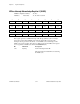
VXIbus A24/A32 Registers
Some of the registers on the VXI-MXI-2 are accessible only within the A24 or A32 space
that the Resource Manager allocates to the VXI-MXI-2. The following are register
descriptions of some of these registers. See Table 5-2 for a register map of these registers.
The table gives the mnemonic, offset from the base address, access type (read only, write
only, or read/write), access size, and register name.
These registers occupy the first 4 KB of address space allocated to the VXI-MXI-2. Any
access to the VXI-MXI-2 A24/A32 space beyond the first 4 KB (address offsets above
FFF hex) will map to the onboard DRAM SIMM sockets. The address offset shown in
each register description is the offset from the base A24/A32 address of the VXI-MXI-2
as defined by the VIDR and VOR registers.
Most of these registers are used to configure the two onboard DMA controllers. The two
DMA controllers are identical to each other but are independent; they can be used
simultaneously without affecting the operation of each other. Because the registers for the
two DMA controllers are identical, this section describes only one set of registers, but the
descriptions apply to both DMA controllers. The registers for DMA Controller 1 begin at
offset D00 from the VXI-MXI-2 module base A24/A32 address, while the registers for
DMA Controller 2 begin at offset E00 as shown in Table 5-2. For an example of how to
use the DMA controllers, refer to Appendix F, DMA Programming Examples.