
User manual


Chapter 5 Register Descriptions
© National Instruments Corporation 5-75 VXI-MXI-2 User Manual
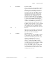
DMA Source Address Register (SARx)
SAR1 VXIbus A24 or A32 Offset: D10 (hex)
SAR2 VXIbus A24 or A32 Offset: E10 (hex)
Attributes: Read/Write 32, 16, 8-bit accessible
31 30 29 28 27 26 25 24
SA[31] SA[30] SA[29] SA[28] SA[27] SA[26] SA[25] SA[24]
23 22 21 20 19 18 17 16
SA[23] SA[22] SA[21] SA[20] SA[19] SA[18] SA[17] SA[16]
15 14 13 12 11 10 9 8
SA[15] SA[14] SA[13] SA[12] SA[11] SA[10] SA[9] SA[8]
76 54 321 0
SA[7] SA[6] SA[5] SA[4] SA[3] SA[2] SA[1] SA[0]
This register stores the base address to be used for the source.
Bit Mnemonic Description
31-0 SA[31:0] Source Address
These bits store the address used to access the
source. The value of these bits is modified after
each successful data transfer to the source during
the DMA operation, according to the ASCEND
bit in the DMA Source Configuration Register
(SCRx). If the initial value of these bits is not
aligned to the transfer size indicated by the
TSIZE[1:0] bits in the SCRx, the DMA
controller performs smaller transfers until
address alignment occurs. However, if 64-bit
data transfers are used for the source, this
register must be programmed with an address
divisible by 8. In the case that the DMA
controller terminates due to an error with the
source transfers, these bits would indicate the
address that caused the error. When the source is
DRAM onboard the VXI-MXI-2, these bits must
be programmed with the offset of the source
location within the VXI-MXI-2 module’s
address space, not the VXIbus address of the