
User manual


Chapter 6 System Configuration
VXI-MXI-2 User Manual 6-10 © National Instruments Corporation
Into VXIbus
Mainframe #3
FF-F0
EF-E0
DF-D0
CF-C0
BF-B0
AF-A0
9F-90
8F-80
7F-70
6F-60
5F-50
3F-30
2F-20
4F-40
1F-10
0F-00
VXIbus Mainframe #1
VXIbus Mainframe #6
VXIbus Mainframe #3
VXIbus Mainframe #4
VXIbus Mainframe #5
VXIbus Mainframe #2
Device A
Device B
MXIbus #1
MXIbus #3
MXIbus #2
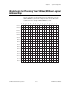
FEDCBA9876543210
Figure 6-6. Logical Address Map Diagram for Example VXIbus/MXIbus System
The multiframe RM by definition is located at logical address 0;
therefore, the host device of the multiframe RM must be assigned a
range of logical addresses that includes logical address 0. Starting
with the MXIbus link on Level 1, which requires the most logical
addresses, assign the lowest available address range of the logical
address map and continue with the next largest MXIbus link.
For the example system, VXIbus Mainframe #1, the host to the
multiframe RM, requires 16 logical addresses and must have a
range that includes logical address 0. It is assigned address range 0
to F hex. The largest first-level MXIbus link is MXIbus #1. It
requires 128 logical addresses, which is one-half of the total
logical address space. The lowest available address range of 128
divisible by a power of two is 80 to FF hex, which is the upper half
of the logical address space. The other first-level MXIbus link,
MXIbus #2, needs only eight logical addresses. It is assigned the
lowest available range of size 8: 10 to 17 hex.