
User manual


Chapter 5 Register Descriptions
VXI-MXI-2 User Manual 5-2 © National Instruments Corporation
to the offset of the register, while the lower eight bits are accessed during an 8-bit cycle
to the offset of the register plus 1.
A square is used to represent each bit. Each bit is labeled with a name inside its square.
An asterisk (*) after a bit name indicates that the bit is active low.
VXIbus Configuration Registers
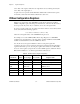
Table 5-1 is a register map of the VXI-MXI-2 register subset, which is accessible in
VXIbus configuration space. The table gives the mnemonic, offset from the base address,
access type (read only, write only, or read/write), access size, and register name.
To access a register in A16 space, the offset given must be added to a base address which
can be derived from the following equation:
base address = C000 hex + (40 hex
*
LA)
where LA is the logical address of the VXI-MXI-2 being accessed.
For example, to access the VDTR (VXIbus Device Type Register) on a VXI-MXI-2
configured to be Logical Address 1, the base address would be C040 hex and the VDTR
would be located at C042 hex, since the VDTR is at offset 2.
Use only the access sizes given in Table 5-1 when accessing each register. For
convenience, the access size is repeated in each register description. Because the table is
organized with 16 bits per row, accessing any register with a 32-bit access will actually
access two of the registers (except in the case of the VIARx registers). Check the Access
Size column in Table 5-1 to see which registers allow 32-bit accesses.
Table 5-1. VXI-MXI-2 VXIbus Configuration Register Map
Mnemonic
Offset
(Hex) Access Type Access Size Register Name
VIDR 0 Read Only 32/16/8 bit VXIbus ID
VDTR 2 Read Only 16/8 bit VXIbus Device Type
VSR/
VCR
4 Read Only/
Write Only
32/16/8 bit VXIbus Status/
VXIbus Control
VOR 6 Read/Write 16/8 bit VXIbus Offset
VMIDR 8 Read/Write 16/8 bit VXIbus MODID
VWR0 A Read/Write 16/8 bit Extender LA Window