
User manual


Chapter 5 Register Descriptions
VXI-MXI-2 User Manual 5-10 © National Instruments Corporation
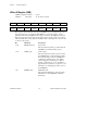
VXIbus Offset Register (VOR)
VXIbus Configuration Offset: 6 (hex)
Attributes: Read/Write 16, 8-bit accessible
15 14 13 12 11 10 9 8
OFFSET[15] OFFSET[14] OFFSET[13] OFFSET[12] OFFSET[11] OFFSET[10] OFFSET[9] OFFSET[8]
76 54 321 0
OFFSET[7] OFFSET[6] OFFSET[5] OFFSET[4] OFFSET[3] OFFSET[2] OFFSET[1] OFFSET[0]
This register determines the base address on the VXIbus and the MXIbus at which to
locate the VXI-MXI-2 module’s A24/A32 resources. This register conforms to the
VXIbus specification.
Bit Mnemonic Description
15-0 OFFSET[15:0] VXIbus Offset
These bits define the A24 or A32 base address at
which the VXI-MXI-2 will locate its registers
and memory. These bits correspond to VXIbus
address lines 23 through 8 when the VXI-MXI-2
is configured for A24, and address lines 31
through 16 when configured for A32. The
REQMEM[3:0] bits in the VXIbus Device Type
Register (VDTR) determine the size of the
VXI-MXI-2 module’s VXIbus memory space by
controlling how many bits of OFFSET[15:0] are
used. The VXI-MXI-2 module’s A24/A32
Decoder compares the REQMEM[3:0] + 1 most
significant bits of OFFSET[15:0] to their
corresponding address lines and responds to
cycles that match. The remainder of the
OFFSET[15:0] bits are ignored. These bits are
cleared by a hard reset and are not affected by a
soft reset.