
User`s manual
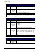

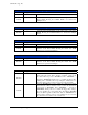
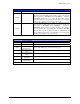

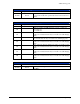


Table Of Contents

VXI Technology, Inc.
48 SM8000 Series Programming
MODULE REGISTERS - SM8000 SERIES CONTROLLER - A24 / A32 - EXTENDED MEMORY
This module is assigned 1 k (1024) bytes of memory as shown in the SMIP II
Configuration/Relay Register Map for A24/A32 address space. The upper 512 bytes of memory
space are unused. The lower 512 bytes of memory are split in half, and form the standard module
configuration and relay registers. The following describes these registers.
Control Register – Read and Write
ADDR
Plug-In LA+0x100
D15
Reset
Module 4
0 = Normal operation
1 = Optical module reset
Resets the optical module located at module base address plus 8h.
See Typical Optical Multi Switch Operation.
D14
Reset
Module 3
0 = Normal operation
1 = Optical module reset
Resets the optical module located at module base address plus 6h.
See Typical Optical Multi Switch Operation.
D13
Reset
Module 2
0 = Normal operation
1 = Optical module reset
Resets the optical module located at module base address plus 4h.
See Typical Optical Multi Switch Operation.
D12
Reset
Module 1
0 = Normal operation
1 = Optical module reset
Resets the optical module located at module base address plus 2h.
See Typical Optical Multi Switch Operation.
D11-D10 Unused
D9
Relay Data Read
Back Polarity Bit
0 = Normal polarity relay data is read back from this module
1 = Inverted polarity relay data is read back from this module
Pon state = 0
This bit may be used to invert the relay data read back from the
plug-in module. Control, Delay, and Status Register read backs are
not effected by this bit.
D8
ACFAILN Enable
Bit
0 = ACFAILN is enabled to reset this module's relays
1 = ACFAILN is disabled from resetting this module's relays
Pon state = 0