
Data Sheet


we-online.com
Würth Elektronik eiSos GmbH & Co. KG - Data Sheet - REV 1.0
17/31
WPMDH1102401 / 171012401
MagI³C Power Module
VDRM - Variable Step Down Regulator Module
DESIGN FLOW
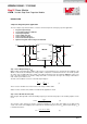
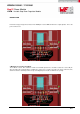
Power Loss [W]
Output Current [A]
Power Loss: V
OUT
= 12V @ T
AMB
= 85°C
0.0
0.3
0.6
0.9
1.2
1.5
0.0 0.2 0.4 0.6 0.8 1.0
V
IN
= 15V
V
IN
= 24V
V
IN
= 36V
From the graph we read a power loss of 0.75W. Entering the values in formula (19) results in:
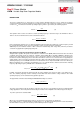
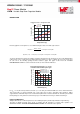
To achieve this thermal resistance the PCB is required to dissipate the heat effectively. The area of the PCB will have
a direct effect on the overall junction-to-ambient thermal resistance. In order to estimate the necessary copper area
we can refer to the following package thermal resistance graph. This graph is taken from the “TYPICAL
PERFORMANCE CURVES“ section and shows how the
varies with the PCB area.
Thermal Resistance θ
JA
[°C/W]
Board Area [cm²]
Package Thermal Resistance θ
JA
4 Layer
Printed Circuit Board with 35µm Copper
0LFM (0m/s) air
225LFM (1.14m/s) air
500LFM (2.54m/s) air
Evaluation Board Area
0
5
10
15
20
25
30
35
40
0 10 20 30 40 50 60
For
and only natural convection (i.e. no air flow), the minimum PCB area can be smaller than 9cm
2
.
This corresponds to a square board with 3cm x 3cm copper area, 4 layers, and 35µm copper thickness. Higher
copper thickness will further improve the overall thermal performance. Note that thermal vias should be placed under
the IC package to easily transfer heat from the top layer of the PCB to the inner layers and the bottom layer.
Light Load Operation:
At light load the device continuously decreases the switching frequency and thereby maintains a high efficiency.
The ripple is slightly increasing in this mode of operation but still small due to no burst mode operation. See
waveforms in section “TYPICAL PERFORMANCE CURVES”. No minimum load is required.