
Data Sheet


WPMDH1152401 / 171012402
MagI
3
C Power Module
VDRM – Variable Step Down Regulator Module
we-online.com Würth Elektronik eiSos GmbH & Co. KG – Data Sheet Rev. 2.0
© December 2017
30/54
DETERMINE POWER LOSSES AND THERMAL REQUIREMENTS OF THE BOARD
This section provides an example of calculation of power losses and thermal design of the board.
As a starting point the following application conditions can be considered:
V
IN
=24V, V
OUT
=12V, I
OUT
=2A, T
A(MAX)
=85°C and T
J
MAX
=125°C
where T
A
is the maximum air temperature surrounding the module and T
J(MAX)
is the maximum value of the junction
temperature according to the limits in the “OPERATING CONDITIONS” section on page 4.
The goal of the calculation is to determine the characteristics of the required heat sink. In the case of a surface mounted
module this would be the PCB (number of layers, copper area and thickness). These characteristics are reflected in the
value of the case to ambient thermal resistance (
).
The basic formula for calculating the operating junction temperature T
J
of a semiconductor device is as follows:
T
J
=P
IC-LOSS
θ
JA
+ T
A
(19)
P
IC-LOSS
are the total power losses within the module´s IC and are related to the operating conditions.
Ɵ
JA
is the junction to ambient thermal resistance and calculated as:
θ
JA
=θ
JC
+θ
CA
(20)
Ɵ
JC
is the junction to case thermal resistance.
Combining equations (19) and (20) results in the maximum case-to-ambient thermal resistance:
θ
CA(MAX)
<
T
J(MAX)
-T
A(MAX)
P
IC-LOSS
- θ
JC
(21)
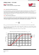
From section ”THERMAL SPECIFICATIONS“ (page 4) the typical thermal resistance from junction to case (
) is defined as
1.9 °C/W. Use the 85°C power dissipation curves in the “TYPICAL PERFORMANCE CURVES“ section (page 12) to
estimate the P
IC-LOSS
for the application being designed.
0,00
0,20
0,40
0,60
0,80
1,00
1,20
1,40
1,60
1,80
2,00
2,20
0 0,25 0,5 0,75 1 1,25 1,5 1,75 2
Power Dissipation [W]
Output Current [A]
171012402 V
IN
= 24V, f
SW
=500kHz, T
A
= 85°C
Vout = 12V
Vout = 5V
2.10W