
Data Sheet


WPMDH1152401 / 171012402
MagI
3
C Power Module
VDRM – Variable Step Down Regulator Module
we-online.com Würth Elektronik eiSos GmbH & Co. KG – Data Sheet Rev. 2.0
© December 2017
31/54
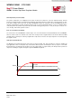
From the graph a power loss of 2.10W is read. Entering the values in formula (21) results in:
θ
CA(MAX)
<
125°C-85°C
2.10W
-1.9°C/W=17.2°C/W
θ
JA(MAX)
=θ
JC
+ θ
CA(MAX)
=1.9°C/W+17.2°C/W= 19.1°C/W
To achieve this thermal resistance the PCB is required to dissipate the heat effectively. The area of the PCB will have a
direct effect on the overall junction-to-ambient thermal resistance. In order to estimate the necessary copper area, the
following thermal resistance graph for the package should be considered.
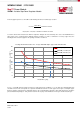
For
< 19.1°C/W and only natural convection (o LFM, Linear Feet per Minute, i.e. no air flow), the minimum PCB area
should be 37.5cm
2
. This corresponds to a square board with about 6.1cm x 6.1cm copper area, 4 layers, and 35µm copper
thickness. Higher copper thickness will further improve the overall thermal performance. Note that thermal vias should be
placed under the IC package to easily transfer heat from the top layer of the PCB to the inner layers and the bottom layer.
0
5
10
15
20
25
30
35
40
0 10 20 30 40 50 60
Thermal Resistance
θ
JA
[°C/W]
Board Area [cm²]
Package Thermal Resistance θ
JA
- 4 Layer PCB with 35µm copper and 36 thermal vias
0LFM (0 m/s) air
225LFM (1.14 m/s) air
500LFM (2.54 m/s) air
19.1
37.5