
Data Sheet


WPMDH1152401 / 171012402
MagI
3
C Power Module
VDRM – Variable Step Down Regulator Module
we-online.com Würth Elektronik eiSos GmbH & Co. KG – Data Sheet Rev. 2.0
© December 2017
39/54
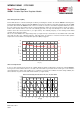
LAYOUT RECOMMENDATION
PCB layout is an important part of DC-DC converter design. Poor board layout can disrupt the performance of a DC-DC
converter and surrounding circuitry by contributing to EMI, ground bounce and resistive voltage drop in the traces. These
can send erroneous signals to the DC-DC converter resulting in poor regulation or instability. A good layout can be
implemented by following simple design rules.
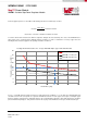
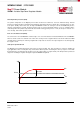
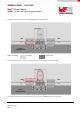
1: Minimize the area of switched current loops.
C
IN
VIN
PGND
VOUT
Power Module
C
OUT
Loop 1
Loop 2
High
di/dt
V
IN
V
OUT
GND
GND
The target is to identify the paths in the system that have discontinuous current flow. They are the most critical ones
because they act as an antenna and cause observable high frequency noise (EMI). The easiest approach to find the critical
paths is to draw the high current loops during both switching cycles and identify the sections which do not overlap. They are
the ones where no continuous current flows and high di/dt is observed. Loop1 is the current path during the ON-time of the
high-side MOSFET. Loop2 is the current path during the OFF-time of the high-side MOSFET.
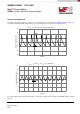
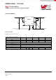
V
IN
VIN
FB
PGND
VOUT
Module
R
FBT
R
FBB
C
OUT
AGND
6
7
C
IN
1
EP 4
V
OUT
GND
GND
Based on those considerations, the path of the input capacitor C
IN
is the most critical one to generate high frequency noise
on V
IN
. Therefore place C
IN
as close as possible to the MagI³C power module V
IN
and PGND exposed pad EP. This will
minimize the high di/dt area and reduce radiated EMI. Additionally, grounding for both the input and output capacitor should
consist of a localized top side plane that connects to the PGND exposed pad.