
Data Sheet

WPMDH1152401 / 171012402
MagI
3
C Power Module
VDRM – Variable Step Down Regulator Module
we-online.com Würth Elektronik eiSos GmbH & Co. KG – Data Sheet Rev. 2.0
© December 2017
42/54
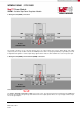
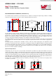
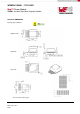
4: Connection to VIN
C
IN1
C
IN2
C
OUT1
C
OUT2
V
IN
GND
GND
V
OUT
1
2
4
3
5 6
7
VIN
RON
EN
AGND
SS
FB
VOUT
R
ON
C
SS
R
FBT
R
FBB
C
FF
PGND
MagI
3
C Module
Bottom
GROUND PLANE
R
ENT
R
ENB
In order to avoid noise injection into RON pin, the resistor R
ON
should be routed to one of the input capacitors.
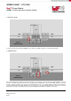
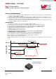
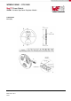
5: Feedback layout
C
IN1
C
IN2
C
OUT1
C
OUT2
V
IN
GND
GND
V
OUT
1
2
4
3
5 6
7
VIN
RON
EN
AGND
SS
FB
VOUT
R
ON
C
SS
R
FBT
R
FBB
C
FF
PGND
MagI
3
C Module
Bottom
GROUND PLANE
R
ENT
R
ENB
The resistor divider (R
FBT
and R
FBB
) should be located close to the FB pin. Since the FB node is high impedance, the trace
thickness should be kept small. The traces from the FB pin to the middle point of the resistor divider should be as short as
possible. The upper terminal of the output resistor divider (where the V
OUT
is normally applied) should be connected to the
positive terminal of the last output capacitor (C
OUT2
), because this is the node with the lowest noise. The traces from R
FBT
,
R
FBB
and C
FF
should be routed away from the body of the MagI³C Power Module to minimize noise pickup.