
Data Sheet

WPMDH1152401 / 171012402
MagI
3
C Power Module
VDRM – Variable Step Down Regulator Module
we-online.com Würth Elektronik eiSos GmbH & Co. KG – Data Sheet Rev. 2.0
© December 2017
45/54
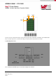
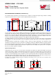
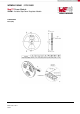
EVALUATION BOARD SCHEMATIC (178012402 v3.0)
The evaluation board schematic has been developed to be suitable for all input and output voltage conditions, switching
frequencies and load currents as well as to achieve optimum load transient response.
R
ON
C2
RON
VIN
EN PGND SS
FB
VOUT
Module
R
FBT
R
FBB
C
SS
C
FF
C4
AGND
1
2
3
EP
5
4
6
7
R
ENT
R
ENB
C5
V
IN
V
OUT
IC1
Cf
C6
R19
Lf
C3
GND GND
+
C1
+
C7
Optional input filter
Optional
Optional
The two multi-layer ceramic capacitors (MLCCs) C2 and C3 at the input handle the switching current ripple and support fast
load transients preventing the voltage at the VIN pin from dropping, potentially below the UVLO threshold. Two MLCCs in
parallel helps to reduce the ESR. The additional aluminum electrolytic capacitor C1 is only for evaluation board protection
purpose. It is mounted as termination of the supply line and provides a slight damping of possible oscillations of the series
resonance circuit represented by the inductance of the supply line and the input capacitance.
The additional MLCC Cf is part of the input filter and is mounted on the board. The inductor Lf instead is not mounted and
replaced by the zero ohm resistor R19. In case the input filter is placed, R19 must be removed and an appropriate Lf
mounted.
The output capacitors should provide a low ESR, in order to reduce the output voltage ripple. The requirement of high
capacitance for good transient response performance is fulfilled by mounting an additional aluminum electrolytic capacitor
C7 in parallel to the MLCC output capacitors. The use of three MLCCs in parallel leads to a very low total ESR. Furthermore,
the use of more MLCCs in parallel at the input and at the output increases the reliability of the system (in case one capacitor
fails, there are still two capacitors remaining).
Operational Requirements
At high duty cycles (V
IN
very close to V
OUT
) the input current will be very similar to the output current. Make sure that your
supply for the module is capable of delivering high enough currents (check the current limit setting of your power supply). In
case your module output voltage V
OUT
is set to very low values (for example 0.8V) electronic loads might not be able to work
correctly. Use discrete high power resistors instead as a load. Use thick and short leads to the input of the module and to the
load. High currents result in additional voltage drops across the cables which decrease the voltage at the load. Measure the
input and output voltage directly at the ceramic capacitors at the input and output (test points).
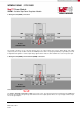
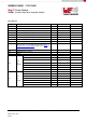
In order to have a constant switching frequency of 500kHz, put the jumper of R
ON
on the same line of the jumper of the
selected V
OUT
(see below).
90k9
75k0
49k9
37k4
27k4
18k2
ADJ
6V
5V
3.3V
2.5V
1.8V
1.2V
ADJ
RON
selection
V
OUT
selection
That corresponds to f
SW
= 500kHz
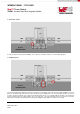
90k9
75k0
49k9
37k4
27k4
18k2
ADJ
6V
5V
3.3V
2.5V
1.8V
1.2V
ADJ
RON
selection
V
OUT
selection
That DOES NOT correspond to f
SW
= 500kHz