
Data Sheet


we-online.com
Würth Elektronik eiSos GmbH & Co. KG - Data Sheet - REV 1.0
13/25
WPMDM1500602/ 171050601
MagI³C Power Module
VDRM - Variable Step Down Regulator Module
DESIGN FLOW
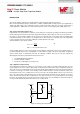
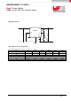
Step 7. Optional: Synchronization to an external clock
The PWM switching frequency can be synchronized to an external frequency source. If this feature is not used,
connect this input either directly to ground, or connect to ground through a resistor of 1.5kΩ ohm or less. The allowed
synchronization frequency range is 650kHz to 950 kHz. The typical input threshold is 1.4V transition level. Ideally the
input clock should overdrive the threshold by a factor of 2, so direct drive from 3.3V logic via a 1.5kΩ source
resistance is recommended. Note that applying a sustained “logic 1” corresponds to zero hertz PWM frequency and
will cause the module to stop switching.
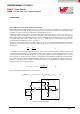
Determine power losses and thermal requirements of the board
For example:
the device must see a maximum junction-to-ambient thermal resistance of:
(10)
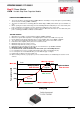
Given the typical thermal resistance from junction to case to be 1.9°C/W. Use the 85°C power dissipation curves in
the typical performance characteristics section to estimate the P
IC-LOSS
for the application being designed. In this
application it is 5.5W.
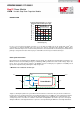
0 1 2 3 4 5
V
IN
= 9V
V
IN
= 12V
V
IN
= 24V
V
IN
= 36V
Power Loss [W]
Output Current [A]
Power Loss: V
OUT
= 3.3V @ T
AMB
= 85°C
0
1
2
3
4
5
6
7
8
To achieve this thermal resistance the PCB is required to dissipate the heat effectively. The area of the PCB will have
a direct effect on the overall junction-to-ambient thermal resistance. In order to estimate the necessary copper area
we can refer to the following package thermal resistance graph. This graph is taken from the typical performance
characteristics section and shows how the
varies with the PCB area.