Modular I/O System INTERBUS S Manual Technical description, installation and configuration 750-132 Version 2.2.
ii • General Copyright ã 1997-2001 by WAGO Kontakttechnik GmbH All rights reserved. WAGO Kontakttechnik GmbH Hansastraße 27 D-32423 Minden Phone: +49 (0) 571/8 87 – 0 Fax: +49 (0) 571/8 87 – 1 69 E-Mail: info@wago.com Web: http://www.wago.com Technical Support Phone: +49 (0) 571/8 87 – 5 55 Fax: +49 (0) 571/8 87 – 4 30 E-Mail: support@wago.com Every conceivable measure has been taken to ensure the correctness and completeness of this documentation.
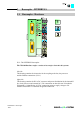
TABLE OF CONTENTS • iii TABLE OF CONTENTS Section 1: Explanations Section 2: System Description INTERBUS S, Configuration, Initial Starting, Diagnosis Section 3: Digital Inputs 750-400, 750-401, 750-402, 750-403, 750-405, 750-406, 750-410, 750-411, 750-408, 750-409, 750-412, 750-413, 750-414, 750-415 750-404 Section 4: Digital Outputs 750-501, 750-502, 750-504, 750-516, 750-519 750-506 750-509 750-511 750-512, 750-513, 750-514, 750-517 Section 5: Analog Inputs 750-452, 750-454, 750-482, 750-484 75
iv • Notes Modular I/O System INTERBUS S
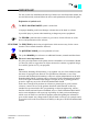
IMPORTANT! For fast, trouble free installation and start up of the devices described in this manual, the user should carefully read and follow the advice and explanations offered in this guide. Explanation of symbols used: The EXCLAMATION POINT symbol is used when: a) improper handling could cause damage or destruction of the hard- or software b) possible injury to persons when interfacing to dangerous process peripherals.
Table of contents chapter 2 1 The WAGO I/O SYSTEM 1 2 Buscoupler Interbus S 2 2.1 Buscoupler-Hardware 2.2 Supply voltage - Electronics 2.3 Supply voltage - Field Side 2.4 Bus connection and station address 2 3 4 5 3 Enclosure and technical data 8 4 Interbus S 9 4.1 Interface Modules 4.2 Configuration software 9 10 5 Configuration of the fieldbus node in the master controller 11 5.1 Identification code 5.2 ID Code for WAGO I/O System 5.3 IBS CMD Software 5.
1 The WAGO I/O System The WAGO I/O SYSTEM consists of various components which are capable of providing modular and application specific fieldbus nodes for various fieldbusses. I11.1 Setting up a fieldbus node with the WAGO I/O SYSTEM General remark: A fieldbus node consists in principle of a fieldbus coupler at the front end, a number of special function modules and a termination module which is placed at the other end.
Assembly of the WAGO I/O System All components of the system can be snapped directly on a carrier rail according to EN 50022 (DIN 35). When snapping the analog or digital components onto the rail, no special sequence must be observed. The secure positioning and connection of the individual function modules and the coupler is provided by a snap-in system. This snap-in system provides automatic interlocking onto the DIN rail assembly.
The clamping force adjusts automatically to the conductor cross section. The flat clamping face of the CAGE CLAMP spring presses the conductor against the current bar without damage. Any deformation or movement of the conductor is compensated, thus eliminating the risk of a loose connection. The contact point between conductor and CAGE CLAMP is well protected against corrosive deterioration. This connection is made fast and, furthermore, it is maintenance-free.
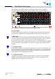
2 Buscoupler - INTERBUS S 2.1 Buscoupler - Hardware Ill. 2: The INTERBUS buscoupler The 750-304 Interbus coupler consists of two major electronic sub systems: left side: This housing contains the electronics for the coupling to the bus, the processor and the fieldbus connection. (ill. 2.1) right side: This housing contains the DC to DC converter and power distribution for the internal K bus, local processor and external 24 V DC connections to other discrete I/O modules. Illustration 2.
2.2 Supply Voltage - Electronics Ill. 3: Termination points for the power supply and the internal electronics The nominal operating voltage of the Buscoupler and the control electronics in the function modules is 5 V DC. The supply is connected to the first two CAGE CLAMPS at the top of the coupler as seen in Ill. 3. The 24 V DC supply voltage is generated by an internal voltage regulator (DC/DC converter) and fed to the electronics (5 V DC).
2.3 Supply Voltage - Field Side Ill. 4: Termination points for the supply voltage - Field side The connection of the supply voltag e is electrically isolated from the internal electronics. Two CAGE CL AMPS are alway s connected by a power contact. By this way, the power supply is taken to different points of the configuration. It is possible to supply the following at the termination points (Ill.
When using the supply module 750-601/602, the field supply from the bus coupler is interrupted. From that point a new power supply connection is necessary to provide DC to any additional I/O modules. WARNING! The ground ( earth) field side contact should be disconnected when testing the isolation. Otherwise the results could be wrong or even the module could be destroyed.
2.4 Bus connection and station (node) address Ill. 5: Bus connection Fieldbus connection: The Interbus interface is normally provided by D SUB connection according Standard EIA RS485 for data transmission by wires.
Configuration Interface The configuration interface used for the communication with WAGO-I/O-CHECK or for firmware upload is located behind the cover flap. Configuration interface Fig. X-1: Configuration interface g01xx06e The communication cable (750-920) is connected to the 4-pole header.
3 The Enclosure and Specifications SYSTEM DATA: Number of function modules Number of I/O points Transmission medium max. bus length Baud rate INTEBUS S / Enclosure and specifications 750-304 750-324 256 on request 4096 on request shielded Cu-cable (5 x 0.
TECHNICAL DATA: Number of function modules Digital peripheral signals Analog peripheral signals Configuration possibility Bus connection Voltage supply Input current Internal current Power jumper contacts Maximum current supplied to K-Bus for internal module use Voltage power jumper contacts Current power jumper contacts Data contacts 750-304 750-324 dig.+analog digital 64 32 256 64 32 --via PC or control --2 D-SUB with protection against vibration 24V DC (-15%/+20%) 105 mA typ; 900 mA max. 85 mA typ.
Interbus S buscoupler with extended diagnostics 750-304/000-001 The Interbus S buscoupler with no. 750-304/000-001 has the possibility of extented diagnostic functions. The technical data is the same as 750-304. Different from the standard buscoupler, a word for diag nostic messages is put into the input data process image and a word for the control of the diag nostic input is put into the output data process image.
4 INTERBUS S The Interbus S system (DIN 19245 part 1.2) is set up as a data ring with a central master slave access procedure. All modules are understood as one log ical module. Each partner receives data at its input and sends it to the nex t partner at its output. There is no addressing with a data frame because each partner knows by special control sig nals (CLOCK, RESET, SELECT, CONTROL) where it is placed in the ring. So there is no bus address.
4.2 Configuration software In order to make the connection between a PLC or PC and the remote stations, the master cards must be configured with the individual station data. For this, the following software packages are available.
5 Configuration of the fieldbus node in the master 5.1 Identification Code In the ID cycle which is carried out for the initialization of the Interbus system, the users connected users are identified by their function and their byte length. The Interbus S coupler identifies its length after being started in the initialization phase of the bus modules and forms a corresponding ID code. To this effect each slave has an implemented identification register (ID register) comprising 2 bytes.
5.2 ID Code for WAGO I/O System Due to the combined use of dig ital, analog and special functions on one fieldbus station and with the given structure of the I nterbus ID codes, it is impossible to manag e with one ID code.
5.3 IBS CMD configuration software In the following chapter the configuration package IBS CMD configuration software is presented in short form. This procedure facilitates operation of the WAGO Interbus buscoupler. Further and specific information is given in the respective operating instructions of the different software packages. 5.3.1 CMD Software Package Please pay attention that the corresponding interfacing and the function extended should be selected.
1) Automatic configuration Ill. 11: Automatic configuration If the complete fieldbus system with all stations and the master interface is operational, automatic configuration of the connected stations can be called up via the menu „bus structure“. Then the communications are started automatically and the configuration is determined and set.
2) Ident code Ill. 12: Insertion of the WAGO I/O System via the Ident code For manual configuration, the menu item „ bus structure“ in the config uration screen must be selected. You will then see Ill. 12. The corresponding ID code of table 3 and the length of the process data channel must be indicated in the selected submenu. The length is dependent on the module with the largest data length.
Ill. 13: Insertion of the ID code and the data length With the finalization of the entries via the key OK, a menu for the definition of the user will appear.
Ill.
After all data has been entered and stored via OK, the station created with the WAGO Interbus coupler is then integrated into the fieldbus system being set up.
5.4 Example of an application Ill.
The addresses indicated in the table results from the master configuration started in the basic address. By the internal structure of the Interbus coupler, the process image is divided as follows: O0 Output data .... .....word orientated data .... Ox Ox+1 bit orientated data Ox+y Input data I0 .... ....word orientated data .... Ix Ix+1 bit orientated data Ix+y Due to this division, the first addresses allocated in the configuration are reserved for the analog inputs and outputs.
6 Buscoupler startup and troubleshooting After configuration of the master connection and electrical installation of the fieldbus node/station, operation of the system can begin. After power to the B uscoupler and I /O modules has been applied, the B uscoupler verifies all internal functions, components and the communication interface by an internal diagnostic routine. Then the function modules and the existing configuration is determined. At the same time a hidden file is stored.
After elimination of the fault, the buscoupler can only be set to the normal working condition by another POWER ON sequence. The green I/O LED flashes when accessing the I/O modules internal data channels. After being switched on, the buscoupler queries the configuration of the bus modules but does not carry out a data exchange with the I/O modules. This means that the red I/O LED will extinguish after a faultless startup. The green I/O LED will indicate when data is being exchanged by the Interbus network.
7 General conditions This chapter describes the general conditions for error-free running of the :$*2Ç, 2Ç6<67(0 7.1 Transporting and storing conditions The following declarations concern modules which are transported and stored in the original package. Condition Free fall Temperature Relative humidity allowed values ≤ 1m -40° to +70° C 5 to 95% (without condensation) 7.
Test for Oscillations Impulse 7.3 Test sequence Remarks Test for oscillations Type of oscillation: sweep with a rate of IEC 68, part 2-6 change of 1 octave per minute 10 Hz ≤ f < 57 Hz, const. amplitude 0,075mm 57 Hz ≤ f ≤ 150 Hz, const.
7.4 Electromagnetic compatibility Method of measurement Interference with narrow-band conducted disturbance Interference with impulse groups Discharge of static electricity Interference with electromagnetic fields Interference field strength Disturbance EN 50082-2, A EN 50082-2, B EN 50082-2, B EN 50082-2, A EN 55011 These requests for electromagnetic compatibility are fulfilled by all modules of :$*2Ç, 2Ç6<67(0 (except for 750-630 and 750-631). 7.
Digital Inputs (24 V AC/DC, 120 V AC, 230 V AC, 48 V DC) PN: 750-400...415 Technical description The supply is applied by a series-connected termination to each I/O module for the respective operating voltage. Power connections are made automatically from module to module when snapped onto the DIN rail. Attention: The lowest power jumper contact is not carried out for some modules (e.g. 4-channel)! A module which needs all contacts (e.g.
Technical Data: Item Number 750Number of inputs Input filter Nominal voltage Signal voltage (0) Signal voltage (1) Input current (internal) Input current (field side) Isolation Internal bit width Configuration Operating temperature Wire connection Dimensions (mm) WxHxL Item Number 750Number of inputs Input filter Nominal voltage Signal voltage (0) Signal voltage (1) Input current (internal) Input current (field side) Isolation Internal bit width Configuration Operating temperature Wire connection Dimension
Item Number 750Number of inputs Input filter Nominal voltage Signal voltage (0) Signal voltage (1) Input current (internal) Input current (field side) Isolation Internal bit width Configuration Operating temperature Wire connection Dimensions (mm)WxHxL Item Number 750Number of inputs Input filter / Conversion time Nominal voltage Signal voltage (0) Signal voltage (1) Input current (internal) Input current (field side) Isolation Internal bit width Configuration Operating temperature Wire connection Dimensio
Counter modules PN 750-404, 750-404/000-001, 750-404/000-002 750-404/000-003, 750-404/000-004 Up/Down Counter 100 kHz, 750-404 Technical Description: Attention! The description that is in the I/O ring binder data pages (88-530/013-600 dated 7/96) is not correct. The bottom contacts are additional outputs. Attention: The lowest power jumper contact is not carried out for some modules (e.g. 4-channel)! A module which needs all contacts (e.g.
Technical Data: Item Number: 750Number of outputs Output current Number of counter Input current (internal) Nominal voltage Signal voltage (0) Signal voltage (1) Switching rate Output current Counter size Isolation Bit width Configuration Operating temperature Wire connection Size (mm)WxHxD Counter Module 750-404 404, 404/000-001 404/000-004 404/000-002 2 0.5 A 1 70 mA 24 V DC (-15% +20%) -3V.....+5V DC +15V...+30V DC 100 kHz 10 kHz max. 5 mA typ.
Organization of the in- and output data: The counter begins processing with pulses at the CLOCK input. The changes from 0 V to 24 V are counted. The counter counts up, if the input U/D is set at 24 V. With an open circuit input or 0 V the counter counts backwards. The two bottom contacts each include another output. These outputs are activated through bits in the control byte.
An example: The counter is set with “Set Counter” to the value 0x0000.0000 - 0X1X.XXXX, 0x00, 0x00, 0x00, 0x00 are carried over as output value (carry over the control-byte and the new counter position), -wait until the input value is 0X1X.XXXX, 0x00, 0x00, 0x00, 0x00 (the status-byte shows the loading feedback) , -carry over 0x00, 0x00, 0x00, 0x00, 0x00 as output value (release counter). Wait for the first and further counting pulse -the input value is XX00.
Counter with enable input 750-404/000-001 Technical description: The counter module also can be ordered as counter with enable input (750-404/000001). The counter begins processing with pulses at the CLOCK input. The changes from 0 V to 24 V are counted. The counter counts down if the input U/D is set at 24 V. With an open circuit input or 0 V the counter counts up. The data format of the module is 4 bytes data and a control/status byte. The module is a 32 Bit counter. The ID Code os 180 (0xB4).
Peak Time Counter 750-404/000-002 Technical data The counter module also can be ordered as peak time counter with 750-404/000-002. This description is only intended for hardware version X X X X 0 0 0 1- - - -. The serial number can be found on the right side of the module. The counter begins processing with pulses at the CLOCK input. The changes from 0 V to 24 V are counted. The counter counts up if the input U/D is set at 24 V. With an open circuit input or 0 V the counter counts backwards.
Organization of the in- and output data: The counter begins processing with pulses at the CLOCK input for a special time span. The time span is predefined as 10 s. The state of the counter is stored in the processs image until the next period. After the recording the counting starts again at 0. The activation of the counting and the synchronisation with the SPS is made by a handshake in the control and status byte.
Frequency Counter Module, 750-404/000-003 Status CLOCK Status Gate Q2 O1 O2 Q1 G Clk +E2 Clock Gate + + 24V 24V 24V - 0V- 0V 0V power jumper contacts O1 O2 Q1 Q2 S S O1Q1 O2 Q2 750-404 000-003 Technical Description The counter module 750-404/000-003 measures the period of the 24 V DC input sig nal at the CL OCK terminal and converts it into a corresponding frequency value. The measurement is enabled if the GATE terminal is an open circuit input or 0V.
Technical Data: Item-No.: 750Supply Voltage Input Voltage (low) Input Voltage (high) Input Current Min. Pulse Width Output Current Voltage Drop Frequency Range: Integration time = 1 period Integration time = 4 periods Integration time = 16 periods Measuring Error: Range 0.1 - 100 Hz Range 1 - 1000Hz Range 10 - 10000Hz Data Format: Process Image Internal Bit Width Input Current (internal) Operating Temperature Wire Connection Size (mm) WxHxD 404/000-003 24V DC (-15%/+20%) -3V - 5V DC 15V - 30V DC 5mA typ.
Functional description The counter module acquires the time between one or more rising edges of the CLOCK input signal and calculates the frequency of the applied signal. The calculation and process imag e update are initiated every 1st, every 4th or every 16th rising edge depending on the integration time selected via the CONTROL byte. The first detection of a rising edge starts the cy clic period measurement and cannot provide a valid frequency value.
Structure of CONTROL and STATUS byte CONTROL Byte E 5(*B5(4 E E E 79' 5(4 E 6(7B4 E 6(7B4 5(*B5(4 15' :5 5(*B$ 5(*B$ 5(*B$ 5(*B$ E E 5$1*(B6(/ 5$1*(B6(/ 5(4 5(4 5(*B$ 5(*B$ Bit Description 5(*B5(4 5(*B$ $ 79' 5(4 6(7B4 6(7B4 5$1*(B6(/ 5(4 5$1*(B6(/ 5(4 $FFHVV WR WKH UHJLVWHU VWUXFWXUH LV UHTXHVWHG E E FRQWDLQ WKH DGGUHVV RI WKH UHJLVWHU 5HJLVWHU DGGUHVV 5HTXHVW WR FKDQJH WKH PD[LPXP WLPH ZLWKRXW YDOLG GDWD &RQWURO 2XWSXW 4 4 RII
Structure of Input and Output data The input data contain the CL OCK frequency as a binary value. The representation depends on the RANGE_SEL bits in the CONTROL byte. Even the method of measuring is selected via these bits. The following table illustrates the different modes.
Organization of the in- and output data for Interbus Output value of the control unit: Byte D15-D0 D31-D16 D47-D32 Identification Control Byte Output Byte 0 Output Byte 2 Output Byte 1 Output Byte 3 Input value of the control unit: Byte D15-D0 D31-D16 D2D47-D32 Identification Status Byte Input Byte 0 Input Byte 2 Input Byte 1 Input Byte 3 The input-bytes 0 to 3 form the 32 bit counter-output. In the output-bytes 0 to 3 the initial value of the counter can be set.
Digital Outputs (Standard) PN 750-501...504, 516, 519 Technical description: The power supply is provided by a series-connected supply module for the respective operating voltage. Power connections are made automatically from module to module via the internal P.J.C.s when snapped onto the DIN rail. Attention: The lowest power jumper contact is not carried out for some modules (e.g. 4-channel)! A module which needs all contacts (e.g.
Technical Data: Item Number 750Number of outputs Kind of load Nominal voltage Output current (DC) Current consumption (internal) Isolation Internal bit width Configuration Operating temperature Wire connection Dimensions (mm)WxHxL Item Number 750Number of outputs Kind of load Nominal voltage Output current (DC) Current consumption (internal) Isolation Internal bit width Configuration Operating temperature Wire connection Dimensions (mm)WxHxL *) low-side switching Item Number 750Number of outputs Kind of loa
Digital Outputs (Standard with diagnostics) PN 750-506 Technical description: The power supply is provided by a series-connected supply module for the respective operating voltage. Power connections are made automatically from module to module via the internal P.J.C.s when snapped onto the DIN rail. Attention: The lowest power jumper contact is not carried out for some modules (e.g. 4-channel)! A module which needs all contacts (e.g.
Technical Data: Item Number 750Number of outputs Current consumption (internal) Nominal voltage Kind of load Output current (DC) Diagnostics Current consumption (internal) Isolation Internal bit width Configuration Operating temperature Wire connection Dimensions (mm)WxHxL 506 2 15 mA 24V DC (-15%/+20%) resistive, inductive, lamps 0.5 A open circuit, overload 15 mA typ. + load 500 V system / power supply 4 in, 4 out without address or configuration adjustment 0°C....+55°C CAGE CLAMP; 0.08 to 2.
Digital Outputs (Solid State Relay) PN 750-509 Technical Description The power supply for the solid state relay module is connected by a series-connected supply module for the respective operating voltage of 230 V. Power connections are made automatically from module to module via the internal P.J.C.s when snapped onto the DIN rail. Attention: The lowest power jumper contact is not carried out for some modules (e.g. 4-channel)! A module which needs all contacts (e.g.
Technical Data: Item Number 750Number of outputs Current consumption (internal) Switching voltage Switched current Speed of operation Volume resistance Impulse current Overvoltage protection Isolation Internal bit width Configuration Operating temperature Wire connection Dimensions (mm)WxHxL Digital Outputs 750-509 509 2 10 mA 0 V...230 V AC/DC 300 mA AC max. 1.65 ms typ., 5 ms max. 2.1 Ω typ., 3.2 Ω max. 0.5 A (20 s), 1.5 A (0.1 s) >+/- 380 V (suppressor diode) 1.
Pulsewidth Module PN 750-511 Technical Description: This description is for hard and software version X X X number is displayed on the right side of the module. X 2 B 0 2- - - - . The part The initial pre-programmed base frequency is for 250 Hz. The resolution is 10 Bits and the pulsewidth is modulated. Attention: The lowest power jumper contact is not carried out for some modules (e.g. 4-channel)! A module which needs all contacts (e.g.
Technical Data: Part Number 750Number of outputs Current consumption (internal) Nominal voltage Load type Output current Pulse frequency Duty cycle Resolution Isolation Configuration Current Consumption (field side) Internal bit width per channel Operating temperature Wire connections Dimension (mm)BxHxT Preset Frequency Pulsewidth Module 750-511 511 2 70 mA typical (internal) 24V DC (-15% +20%) ohmic, inductive 0.1 A, short circuit protected 1 Hz...20kHz 0%...
Formation of on/off times The programming of the on/off times occur with the resolution of 10 bits. The five LSB of the 16 bit value can be zeros or one. The MSB will hold the sign and is preset to the null state. Duty Cycle % 100 Increments 1023 Binary Value 0111 1111 1111 1111 Hex. 7F FF Dec. 32767 100 1023 0111 1111 1111 0000 7F E0 32752 50 511 0011 1111 1111 1111 3F FF 16383 25 255 0001 1111 1111 1111 1F FF 8191 12.5 127 0000 0001 0000 0000 01 00 256 0.
Process Image Formation for Interbus The process image of the 750-511 appears with 6 by tes of input and 6 by tes of output data.
Digital Outputs (Relay) PN 750-512...514, 517 Technical description: The power supply for the relay coils is not made via the power jumper contacts but directly from the electronics. The respective output contacts of the switching element are therefore always positioned at the field side. Attention: The lowest power jumper contact is not carried out for some modules (e.g. 4-channel)! A module which needs all contacts (e.g.
Technical Data: Item Number 750Type of contact Current consumption (internal) Switching voltage Switching power Switching current Isolation Internal bit width Configuration Operating temperature Wire connection Dimensions (mm)WxHxL Item Number 750Type of contact Current consumption (internal) Switching voltage Switching power Switching current Isolation Internal bit width Configuration Operating temperature Wire connection Dimensions (mm)WxHxL *ohmic load 1) in design Digital Outputs 750-512-514,517
Relays in the modules 750-512 and 750-513: 6ZLWFKLQJ FDSDFLW\ 10 @ $ > W Q H U U X F AC ohmic DC ohmic AC inductive, cosϕ=0.4 1 G H K F W L DC inductive L/R=7ms Z 6 0,1 10 100 1000 6ZLWFKHG YROWDJH >9@ 7\SLFDO HOHFWULFDO OLIHWLPH 1,E+06 V H K F W L Z V I R U H E 30 V DC ohmic 120 V AC ohmic 250 V AC ohmic 30 V DC inductive, L/R = 0.7ms 1,E+05 P X 1 120 V AC inductive, cosϕ=0.
2 Channel Analog Inputs 0-20 mA / 4-20 mA (Differential Inputs) PN 750-452, 454, 750-482, 750-484 Technical Description This description is only intended for hardware version X X X X 2 A 0 0 - - - -. The serial number can be found on the right side of the module. The input channels are differential inputs and they have a common ground potential. The inputs are connected to +I and -I. The shield is connected to „S“. The connection is made automatically when snapped onto the DIN rail.
Technical Data: Item Number 750Number of channels Nominal voltage Current consumption (internal) Voltage Signal current Resistance Resolution Isolation Conversion time Bit width per channel Operating temperature Configuration Wire connection Dimensions (mm)WxHxL Analog Inputs 750-452, 454,482,484 452 2 70 mA 454 482 via system voltage 2 484 70 mA 35 V max. 0-20mA 4-20mA 0-20mA 4-20mA 50 Ω typ. 12 Bit 500 V System/Power supply 2 ms typ. 16 Bit Data, 8 Bit Control/Status 0°C....
The numerical format All analog values will be shown in a unit numerical format. The resolution is 12 Bits. The following table will explain the numerical format. (750-452, 454). The 3 least significant Bits are not taken into account. Input current Input current 0-20 mA 4-20 mA 20 20 0111 1111 1111 1000 Hex. 7F F8 Dec. 32760 10 12 0100 0000 0000 0000 40 00 16384 5 8 0010 0000 0000 0000 20 00 8192 2.5 6 0001 0000 0000 0000 10 00 4096 0.156 4.125 0000 0001 0000 0000 01 00 256 0.01 4.
The numerical format for Siemens In addition to the full 16 bit indication of the measured value it is possible to use the ‘Siemens format’. The measured value is represented by the most significant 12 Bits. The 3 least significant Bits are reserved for diagnostic and status purposes. (750-482, 484) Input current 4-20 mA Binary value > 20 0101 0000 0000 0 20 0101 0000 0000 0 16 Hex. Dec.
Input current 0-20 mA Binary value > 20 0100 0000 0000 0 20 0100 0000 0000 0 10 X : without meaning F : short circuit open circuit Ü : overflow XFÜ 001 Hex. Dec. 40 01 16385 000 40 00 16384 0010 0000 0000 0 000 20 00 8192 5 0001 0000 0000 0 000 10 00 4096 2.5 0000 1000 0000 0 000 08 00 2048 1.25 0000 0100 0000 0 000 04 00 1024 0.625 0000 0010 0000 0 000 02 00 512 0.
2 Channel Analog Inputs +/- 10 V (Differential Inputs) PN 750-456, 750-456/000-001 Technical Description This description is only intended for hardware version X X X X 2 A 0 0 - - - -. The serial number can be found on the right side of the module. The input channels are differential inputs and they have a common ground potential. The inputs are connected to +I and -I. The shield is connected to „S“. The connection is made automatically when snapped onto the DIN rail.
Technical Data: Item Number 750Number of channels Nominal voltage Current consumption (internal) Overvoltage protection Signal voltage Resistance Resolution Isolation Conversion time Bit width per channel Operating temperature Configuration Wire connection Dimensions (mm)WxHxL 456, 456/000-001 2 via system voltage (DC DC converter) 65 mA 35 V max. +/- 10 V 570 kΩ 12 Bit 500 V System/Power supply 2 ms typ. 16 Bit Data, 8 Bit Control/Status 0°C....+55°C none, optional via software parameter CAGE CLAMP; 0.
The numerical format All analog values will be shown in a unit numerical format. The resolution is 12 Bits and the 3 LSBs are not taken into account. The following table will explain the numerical format. Input voltage ±10V > 10 V Status 0111 1111 1111 1111 Hex. 7F FF Dec.
The numerical format for Siemens In addition to the full 16 bit indication of the measured value it is possible to use the Siemens format. The measured value is represented by the most significant 12 Bits. The 3 least significant bits are reserved for diagnostic and status purposes. (750-456/000001). Input voltage ±10V Binary value >10 0111 1111 1111 1 10 0111 1111 1111 1 5 X : without meaning F : short circuit or F : open circuit Ü : overflow XFÜ 001 Hex. Dec.
Input for PT 100 PN 750-461, 750-461/000-002, 750-461/000-003, 750-481 Technical description: This description is only intended for hardware version X X X X 3 A 0 2 - - - -. The serial number can be found on the right side of the module. The described configuration is PT 100. The following description is preliminary and is applicable only to the factory configuration. The inputs are connected to +I and -I. The shield is connected to „S“. The connection is made automatically when snapped onto the DIN rail.
Technical Data: Item Number 750Number of inputs Input current (internal) Voltage supply Sensor types Wire connection Temperature range Resolution Isolation DC/DC Measuring current Bit width per channel Configuration Operating temperature Wire connection Dimensions (mm)WxHxL Presetting 461, 481, 461/000-002, 461/000-003 2 65 mA via system voltage PT100, PT 200, PT 500, PT1000, Ni100, Ni120, Ni1000 2-conductor, 3-conductor (presetting) PT: -200°C..+850°C Ni:-60°C...250°C 0.
The numerical format All temperature values will be shown in a unit numerical format. If the mode ‘DEFAULT’ is selected each bit corresponds to 0.1°C. The possible numerical range refers to the standardized temperature range of the used sensors. The following table will explain the numerical format on a preset PT100. In the third column the numerical format for PT1000 (750-461/000-003) is explained. Temperature °C Voltage (Ohm) >400 Voltage (Ohm) Binary Value 850 390.481 1384,998 100 138.506 25.
The numerical format for 750-461/000-002 All temperature values will be shown in a unit numerical format. Each bit corresponds to 0.1°C. The following table will explain the numerical format for 750-461/000-002. Voltage (Ohm) 10 0000 0000 0110 0100 Hex. 00 64 Dez.
The numerical format for Siemens In addition to the full 16 bit indication of the measured value it is possible to use the ‘Siemens format’. The measured value is represented by the most significant 12 Bits. The 4 least significant Bits are reserved for diagnostic and status purposes. (750-481) Temp. °C Ohm Binary value >400 1111 1111 1111 1 883 400 0111 1111 1111 1 560 300 266 X : without meaning F : short circuit or F : open circuit Ü : overflow XFÜ 001 Hex. Dec.
Input for Thermocouple Modules PN 750-462, 750-469, 750-462/000-XXX Technical description: This description is only intended for hardware version X X X X 2 A 0 1 - - - -. The serial number can be found on the right side of the module. The following description is preliminary and is applicable only to the factory configuration. The shield is connected to „S“. The connection is made automatically when snapped onto the DIN rail. These I/O modules are not provided with integrated power jumper contacts.
Technical Data: Item Number 750Number of inputs Voltage supply Sensor types Cold junction compensation Measuring accuracy Resolution Isolation DC/DC Input current (internal) Bit width per channel Configuration Operating temperature Connection technique Dimensions (mm)WxHxL Presetting 462, 469 2 (differential input, max. +/- 3.5V) via system voltage J, K, B, E, N, R, S, T, U, L, mV Messung on each module <25 µV, typ. 15 µV 0.1°C per Bit 500V system / power supply 65 mA max.
Temperature Ranges of the connectable sensors: L -25°C....+900°C K -100°C...1370°C (Default) J -100°C...+1200°C 750-462/000-006 E -100°C...1000°C 750-462/000-008 T -100°C...+400°C 750-462/000-002 N -100°C...+1300°C 750-462/000-009 U -25°C...+600°C 750-462/000-011 B 600°C...+1800°C 750-462/000-007 R 0°C...+1700°C 750-462/000-010 S 0°C...+1700°C 750-462/000-001 mV-Meter -120 mV...
The numerical formats All temperature values are represented in a uniform numerical format. In the default setting (type K) one Bit corresponds to 0.1°C. The output value corresponds to the temperature range of each sensor as defined according to standards. By using a configuration tool, the output formats can be chosen. The linearization can be switched off and the building of the reference temperature can be switched off also.
2 Channel Analog Input 0-20 mA / 4- 20 mA single ended PN 750-465, 750-466, 750-486, 750-465/000-001 Technical Description This description is only intended for hardware version X X X X 2 A 0 1 - - - -. The serial number can be found on the right side of the module. The input channels are single ended and they have a common ground potential. The inputs are connected to +I. Via 24 V / 0 V a sensor can be provided directly from the module.
Technical Data: Item Number 750Number of channels Nominal voltage Current consumption (internal) Overvoltage protection Signal current Resistance Resolution Isolation Conversion time Bit width per channel Operating temperature Configuration Wire connection Dimensions (mm)WxHxL Analog Inputs 750-465,466,486 465 465/000-001 466 486 2 24 V DC (-15% / +20%) via power jumper contacts 75 mA typ. 0-20mA 35 V max. 4-20mA 50 Ω typ. 12 Bit 500 V system/power supply 2 ms typ.
The numerical format All analog values will be shown in a unit numerical format. The resolution is 12 Bits. The following table will explain the numerical format. (750-465, 466). The 3 LSBs are not taken into account. Input current Input current 0-20mA 4-20mA >20,5 >20,5 0111 1111 1111 1111 Hex. 7F FF Dec.
The numerical format for Siemens In addition to the full 16 bit indication of the measured value it is possible to use the ‘Siemens format’. The measured value is represented by the most significant 12 Bits. The 3 least significant Bits are reserved for diagnostic and status purposes. (750465/000-001). Input Binary value current 0-20mA X : without meaning Hex. F : short circuit or F : open circuit Ü : overflow XFÜ 0100 0000 0000 0 001 4001 Dec.
750-466/000-200 or 750-486: Input Binary value current 4-20mA >20,5 X : without meaning F : short circuit or Hex. Dec.
2 / 4 Channel Analog Inputs 0-10 V single ended PN 750-467, 468, 487, 488 Technical Description This description is only intended for hardware version X X X X 2 A 0 0 - - - -. The serial number can be found on the right side of the module. The input channels are single ended and they have a common ground potential. The inputs are connected to +I and M. The shield is connected to „S“. The connection is made automatically when snapped onto the DIN rail.
Technical Data: Item Number 750Number of channels Nominal voltage Current consumption (internal) Overvoltage protection Signal voltage Resistance Resolution Isolation Conversion time Bit width per channel Operating temperature Configuration Wire connection Dimensions (mm)WxHxL Analog Inputs 750-467,468,487,488 467 2 468 487 488 4 2 4 via system voltage (DC DC converter) 60 mA 60 mA 60 mA 60 mA 35 V max. 0-10 V 133 kΩ typ. 12 Bit 500 V system/power supply 2 ms typ.
The numerical format All analog values will be shown in a unit numerical format. The resolution is 12 Bits. The following table will explain the numerical format. (750-467, 468). The 3 LSBs are not taken into account. Input voltage 0-10V > 10 0111 1111 1111 1111 Hex. 7F FF Dec.
The numerical format for Siemens In addition to the full 16 bit indication of the measured value it is possible to use the ‘Siemens format’. The measured value is represented by the most significant 12 Bits. The 3 least significant Bits are reserved for diagnostic and status purposes. (750-487, 488) Input voltage 0-10V Binary value >10 0101 0000 0000 0 10 0101 0000 0000 0 5 X : without meaning F : short circuit or F : open circuit Ü : overflow XFÜ 001 Hex. Dec.
2 Channel Analog Input 0-20mA / 4-20mA single ended PN 750-472, 750-472/000-200, 750-474, 750-474/000-200 Technical description: This description is only intended for hardware and software version X X X X 0 2 0 2- - -. The serial number can be found on the right side of the module. The input channels are single ended and they have a common ground potential. The inputs are connected to +I. Via 24 V / 0 V a sensor can be provided directly from the module.
Technical Data: Item Number 750- 474 474/000-0200 Number of channels Nominal voltage Overvoltage protection Internal current Input signal Input current Resistance Input voltage Resolution Input filter Noise rejection at sampling frequency 2 24 V DC (-15% / +20%) via power jumper contacts 24 V max. 75 mA typ.
The numerical format The resolution of 750-472 and 750-474 are 15 Bit. Input current Input current Binary value 0-20mA 4-20mA >20,5 >20,5 0111 1111 1111 1111 Dec.
The numerical format for Siemens In addition to the full 16 Bit indication of the measured value it is possible to use the „Siemens format“. The measured value is represented by the most significant 12 Bits. The 3 least significant Bits are reserved for diagnostic and status purpose (750-472/000200, 750-474/000-200). The numerical format for 750-472/000-200 is equivalent to S5 463, 750-474/000-200 equivalent to S5 460/465. Input Binary value current 4-20mA X : without meaning F : short circuit or Hex.
Input Binary value current 0-20mA X : without meaning F : short circuit or F: open circuit Ü : overflow XFÜ 0110 0000 0000 0 001 Hex. Dec.
2-Channel Analog Input ± 10 V, 16 Bit, single ended 0 -10 V, 16 Bit, single ended 750-476 750-478 Function clamp and variants Item-No. 750-476 750-476/000-200 750-478 750-478/000-200 Analog Inputs 750-476, 478 4;13614<<< Description 2-Channel Analog Input ± 10 V, single ended 2-Channel Analog Input ± 10 V, single ended with status infomation within the data word Identification 2 AI ± 10 V DC 16 Bit s.e. 2 AI ± 10 V DC 16 Bit s.e.
Technical description This description is only intended for hardware and software version X X X X 0 4 0 1 - - - - .The serial number can be found on the right side of the module. The input channels are single ended and they have a common ground potential. The inputs are connected to I and 0V. The shield is connected to „S“. The connection is made automatically when snapped onto the DIN rail. Attention: The lowest power jumper contact is not carried out for some modules (e.g.
Technical Data Item Number Number of channels Nominal voltage Overvoltage resistance Internal current consumption Input signal Input impedance Overvoltage protection Resolution Input filter Noise rejection at sampling frequency Noise rejection below sampling frequency Transition frequency Isolation Wandlungszeit Bitwidth per channel Configuration Operating temperature Wire connection Dimensions (mm)WxHxL Analog Inputs 750-476, 478 4;13614<<< 750-476 750-476/000-200 750-478 750-478/000-200 +/- 10 V 0 -
The numerical format All analog values will be shown in a unit numerical format. The resolution for 750-476 and 750-478 is 15 Bit plus sign. 750-476, -478 Input voltage 0-10V ±10V Hex. Dec.
Numerical format with status information For fieldbus master, which evaluates status information in the data word, e.g. from Siemens, a variant of the function clamp is available. The format containes the status in Bit B0 .. B2. The digitalized measuring value is placed at the position Bit B3 .. B15. The numerical format is equivalent to S5 466. 750-476/000-200 Input Value Status LED error voltage Binary Hex. Dec.
Status byte Structure of the status byte: bit meaning • ERROR • Overrange • Underrange Analog Inputs 750-476, 478 4;13614<<< 7 0 6 ERROR 5 4 3 2 res. res. res. res. 1 Overrange 0 Underrange error at the input channel. exceed the allowable measuring range. fall below the allowable measuring range.
2 Channel Analog Outputs 0-10 V PN 750-550, 750-580 Technical Description This description is only intended for hardware version X X X X 2 A 0 1 - - - -. The serial number can be found on the right side of the module. The output signal of 750-550/551 is a 0-10 V signal. Sensors may be connected to „O“ and to the common ground. The shield is connected to „S“. The connection is made automatically when snapped onto the DIN rail. These I/O modules are not provided with integrated power jumper contacts.
Technical Data: Item Number 750Number of channels Nominal voltage Current consumption (internal) Voltage supply Signal voltage Resistance Resolution Isolation Bit width per channel Operating temperature Configuration Wire connection Dimensions (mm)WxHxL 550, 580 2 via system voltage (DC DC converter) 65 mA via system voltage (DC-DC) 0-10 V > 5 kΩ 12 Bit 500 V system/power supply 16 Bit Data, 8 Bit Control/Status 0°C....+55°C none, optional via software parameter CAGE CLAMP; 0.08 to 2.
The numerical format for Siemens In addition to the full 16 bit indication of the measured value it is possible to use the ‘Siemens format’. The measured value is represented by the most significant 12 Bits. The 3 least significant Bits are reserved for diagnostic and status purposes. (750-580) Output voltage 0-10 V > 10 Binary value Hex. Dec. 0101 0000 0000 XXXX 50 01 20481 10 0100 0000 0000 XXXX 40 00 16384 7.5 0011 0000 0000 XXXX 30 00 12288 5 0010 0000 0000 XXXX 20 00 8192 2.
2 -Channel Analog Outputs 0-20 mA / 4-20 mA PN 750-552, 554, 584 Technical Description This description is only intended for hardware version X X X X 2 A 0 1 - - - -. The serial number can be found on the right side of the module. The output signal of 750-552...555, 584 is a 0-10 mA or 4-20 mA signal. Sensors may be connected to „O“ and to the common ground (0V). The shield is connected to „S“. The connection is made automatically when snapped onto the DIN rail.
Technical Data: Item Number 750Number of channels Current consumption (internal) Nominal voltage Signal current Resistance Resolution Isolation Bit width per channel Operating temperature Configuration Wire connection Dimensions (mm)WxHxL 552 554 2 60 mA max. 584 24 V DC (-15% /+20%) via power jumper contacts 0-20mA 4-20mA 4-20mA <500 Ω 12 Bit 500 V system/power supply 16 Bit Data, 8 Bit Control/Status 0°C....+55°C none, optional via software parameter CAGE CLAMP; 0.08 to 2.
The numerical format for Siemens In addition to the full 16 bit indication of the measured value it is possible to use the ‘Siemens format’. The measured value is represented by the most significant 12 Bits. The 4 least significant Bits have no function. (750-584) Output current 4-20 mA 20 Binary value Hex. Dec. 0100 0000 0000 XXXX 40 00 16384 16 0011 0000 0000 XXXX 30 00 12288 12 0010 0000 0000 XXXX 20 00 8192 8 0001 0000 0000 XXXX 10 00 4096 4.
2 Channel Analog Outputs +/- 10 V PN 750-556 Technical Description This description is only intended for hardware version X X X X 2 A 0 1 - - - -. The serial number can be found on the right side of the module. The output signal of 750-556 is a +/- 10 V signal. Sensors may be connected to „O“ and to the common ground (0V). The shield is connected to „S“. The connection is made automatically when snapped onto the DIN rail. These I/O modules are not provided with integrated power jumper contacts.
Technical Data: Item Number 750Number of channels Nominal voltage Current consumption (internal) Signal voltage Resistance Resolution Isolation Bit width per channel Operating temperature Configuration Wire connection Dimensions (mm)WxHxL Analog Outputs 750-556 556 2 via system voltage (DC DC converter) 65 mA +/- 10 V > 5 kΩ 12 Bit 500 V System/Power supply 16 Bit Data, 8 Bit Control/Status 0°C....+55°C none, optional via software parameter CAGE CLAMP; 0.08 to 2.
The numerical format All analog values will be shown in a unit numerical format. The resolution is 12 Bits and the 3 LSBs are ignored. The following table will explain the numerical format. Input voltage +/- 10 V Binary Value 10 Analog Outputs 750-556 0111 1111 1111 1111 Hex. 7F FF Dec. 32767 5 0100 0000 0000 0000 40 00 16384 2.5 0010 0000 0000 0000 20 00 8192 1.25 0001 0000 0000 0000 10 00 4096 0.0781 0000 0001 0000 0000 01 00 256 0.0049 0000 0000 0001 0000 00 10 16 0.
End module, Potential multiplication module, Separation module PN750-600, 750-614, 750-616, 750-616/030-000 Technical Description After the fieldbus node is assembled with the correct buscoupler and selected I/O modules, the end module is snapped onto the assembly. It completes the internal data circuit and ensures correct data flow. The potential multiplication module allows additional + and - voltage connection points (up to 4 additional). This eliminates external terminal blocks.
Separation module Technical description: Use of this module allows increased air- and creepage distances between different field voltages within a node. There are two different types of the separation module. With PN 750-616 you get a module without printing. PN 750-616/030-000 looks like the right one in the above picture. Technical Data: Item No.
Supply modules PN750-601, 602, 609, 610, 611, 612, 613, 615 Technical Description The supply module provides I/O module power through the power jumper contacts. Maximum current supply to all connected modules is 10 A. Maximum current supply to the modules with fuse holder is 6.3 A. Should higher currents be necessary, intermediate supply modules may be added in the assembly. The modules 750-601, 609, 615, 610 and 611 are additionally equipped with a fuse holder.
Technical Data: Item Number 750Voltage 602 24 V DC Current via contacts Operating temperature Wire connection Dimensions (mm) W x H x L internal current 750-613: max. 2 A 601 24 V DC Item Number 750Number of inputs Current consumption Internal bitwidth 610 Voltage Current via contacts Fuse Operating temperature Wire connection Dimensions (mm) W x H x L Supply modules 750-601,602, 609,615,610,611,613 max. 10 A 0 °C ...
Binary spacer module PN 750-622 1XPEHU RI LQSXWV RU RXWSXWV ,QSXWV RU 2XWSXWV :$*2 9 ON 1 23 45 9 Technical description The binary spacer module reserves bit-addresses in the WAGO buscoupler. The number of in or outputs can be chosen by two DIP switches. 2, 4, 6 or 8 bits are possible (1, 2, 3 or 4-channel modules). A third DIP Switch chooses inputs or outputs. The kind of configuration is indicated by means of 3 LEDs even if there is no voltage applied.
Technical Data Item number 750Number of in- or outputs Nominal voltage Internal current consumption Voltage (field side) Current via power jumper contacts Input current (field side) Isolation Internal bit width Configuration Operating temperature Wire connection Dimensions (mm) WxHxL 622 2, 4, 6 or 8 5 V DC internal 10 mA max. 24 V DC (-15%/+20%) 10 A max. 500 V system/power supply 2, 4, 6 oder 8 none, optional via software parameter 0°C....+55°C CAGE CLAMP; 0.08 to 2.
SSI Encoder Interface PN 750-630, 750-630/000-001, 750-630/000-006 Technical Description: This technical description is only valid for hardware and software versions X X X X 2 B 0 2----. The product series number is printed on the right side of the module. The operational mode of the module is factory preset to discern a 24 bit absolute encoder Graycode signal transmitted at 125kHz. The following description is preliminary and is applicable to the factory configuration.
Technical Data: Series 750 Encoder connections Current consumption (internal) Power supply Sensor power supply Baud rate Data field width Signal output (clock) Signal input (positional) Output data format Bit width Configuration Signal isolation Temperature range Wire connection Dimensions (mm) WxHxL Default Configuration SSI encoder 750-630 630 630/000-001 630/000-006 Data Input: D+; D-; Clock Output: CI+; CI85mA typ. 24V DC (-15%/+20%) 24V DC via power jumper contacts max.
Terminal Configuration: Input Signal D+ and Signal DSignal Cl+ and Signal CL+24 V DC 0 V DC Type Input, RS422 Output, RS422 Input Input Function Positional data from encoder, Graycode. Clock signal output for communications interface. 24 V DC supply voltage to module, field connection. 0 V DC supply voltage return to module, field connection.
Organization of the in- and output data for Interbus The module is seen like an analog input with 2 x 16 Bit input data.
Quadrature Encoder Interface PN 750-631, 750-631/000-001 Technical Description: This technical description is only valid for hardware and software versions X X X X 2 B 0 1----. The product series number is printed on the right side of the module. The described operational mode is 4 times or quadrature sampling. The following description is preliminary and is applicable to the factory configuration. Attention: The lowest power jumper contact is not carried out for some modules (e.g.
Technical Data: Series 750Encoder connections Current consumption (internal) Sensor supply voltage Data word Maximum frequency Counter modes Data latch word Commands Supply voltage Current consumption Sensor Bit width Configuration Operational temperature Wire connection Dimensions (mm) WxHxL Default configuration Quadrature Encoder 750-631 631 631/000-001 A, A(inv.); B, B(inv.); Index, Index(inv.
Operational Characteristics: The quadrature encoder interface accepts up to two input signals for the counting increment. The index pulse may also be considered should the control configuration require. There is also a Latch and Gate input available on the module for added functionality. The quadrature encoder provides two signals that are shifted 90 degrees from each other, signals A and B.
The input Latch controls the overtaking of the actual counter value into the Latchregister. This input is activated by teh control bit EN_LATEXT („1“). EN_LACT has to be deactivated („0“). The first change from 0 V to 24 V at the Latch input takes the actual counter value into the Latchregister. The control byte contains the information as listed below.
It is possible to process and/or check the below listed actions via the control and status bits. Extending the 16 bit counting range: The internal counting range is 16 bits or a maximum value of 65535. Should the application require an extended count range the location-difference-integration method may be employed. This method uses the control system to store the interrogated counter value. Any new interrogated value will have the previously stored counter value subtracted from it.
Organization of the in- and output data for Interbus The module is seen like an analog module with 3 x 16 Bit input and output data.
RS232C Interface, TTY Interface -20 mA Current Loop RS485C Interface PN 750-650, 750-651, 750-653, 750-650/000-001 Technical Description: This technical description is only valid for hardware and software versions X X X X 2 C 0 3----. The product series number is printed on the right side of the module. The operational mode described below is the presetting. The following description is preliminary and is applicable to the factory configuration.
Technical Data: Series 750Transmission channel Transmission rate Bit skew Bit transmission Resistance Current consumption (internal) Transmission length Input buffer Output buffer Voltage supply Isolation Bit width internal Configuration Operating temperature Wire connection Dimensions(mm) W x H x L Factory preset Baud rate Bit width internal RS232,TTY,RS485 750-650,651,653 650,650/000-001 651 2 (1/1), T x D and R x D, full duplex 1200 - 19200 baud <3% 2 x 20 mA passive < 500 Ω 50 mA max.
Description of RS 232: The interface module is designed to operate with all WAGO I/O fieldbus couplers. The serial interface module allows the connection of RS 232-Interface devices to the WAGO I/O SYSTEM. The RS 232 Interface module can provide gateways within the fieldbus protocol. This allows serial equipment such as printers, barcode readers, and links to local operator interfaces to communicate directly by the fieldbus protocol with the PLC or PC Master.
Description of TTY: The interface module is designed to operate with all WAGO I/O fieldbus couplers. The TTY interface module allows the connection of TTY-Interface devices to the WAGO I/O SYSTEM. The TTY Interface module can provide gateways within the fieldbus protocol. This allows serial equipment such as printers, barcode readers, and links to local operator interfaces to communicate directly by the fieldbus protocol with the PLC or PC Master. This module supports no higher level of protocol.
Description of RS 485: The interface module is designed to operate with all WAGO I/O fieldbus couplers. The serial interface module allows the connection of RS485 or RS488-Interface devices to the WAGO I/O SYSTEM. The RS485/RS488 Interface module can provide gateways within the fieldbus protocol. This allows serial equipment such as printers, barcode readers, and links to local operator interfaces to communicate directly by the fieldbus protocol with the PLC or PC Master.
Structure of input and output data: The module is a combined analog input and output module with 2 x 16 bit input and output data. The transfer of the data to be transmitted and the received data is made via up to 3 output and 3 input bytes. One control byte and one status byte are used to control the floating data. Requests are indicated by a change of a bit. An assigned bit indicates execution by adopting the value of the request bit.
The PLC is able to control transmission and reception of data by means of the control byte and the status byte.
Examples: The module is initialized. - The initialization bit in the control byte is set. Output byte 0 0x00 Control byte Output byte 2 0000.0100 0x00 Output byte 1 0x00 - After the initialization has been executed, the status byte will give back 000.0100. Input byte 0 XX XX Status byte 0XXX.X0XX 0XXX.X1XX Input byte 2 XX XX Input byte 1 Module is still being reset XX Initialization completed XX Sending of the data string “Hello”: - The first 3 characters and the buffer length of 3 are transmitted.
- As soon as TA = TR, the data has been transferred to the output buffer. Input byte 0 Status byte Input byte 2 Input byte 1 The data is still being transferred. XX 0XXX.XXX1 XX XX Data transfer completed. XX 0XXX.XXX0 XX XX Receiving the character chain “WAGO” - As soon as RA≠RR, the input bytes contain data. Output byte 0 XX Input byte 0 XX ‘W’ (0 x 57) Control yte Output byte 2 0XXX.000X XX Status byte Input byte 2 0XXX.0X0X XX 0011.
Structure of the in and output data for Interbus The module is a combined input and output module with 2 x 16 bit input and output data. Outputs: Word D0 (bit 0-15) D1(bit16-31) Description Output byte0 Output byte2 Control byte Output byte1 Inputs: Word D0 (bit 0-15) D1(bit16-31) Description Input byte0 Input byte2 Status byte Input byte1 The RS232 module is also available with a data format of 5 bytes (item-no. 750650/000-001).
Data exchange module PN 750-654 Technical Description This technical description is only valid for hardware and software versionx X X X X 2 C 0 0 - - - -. The product series number is printed on the right side of the module. The operational mode described below is for the factory preset mode. The following description is preliminary and is applicable to the factory configuration. Many other operational modes are possible (please contact WAGO for the corresponding settings.
Technical Data Series 750- 654 Bit transmission via 2 twisted pair with differential signals 120 Ω Transmission channel Transmission rate Resistance of cable Current Consumption (internal) Transmission length Input buffer Output buffer Voltage supply Isolation Bit width internal Configuration Operating temperature Wire connection Dimensions (mm) W x H x L Factory preset internal bit width Data exchange module 750-654 TxD and RxD, full duplex, 2 channel 62500 Baud 65 mA max. max.
Description of data exchange module The data exchange module allows the exchange of 4 (5) bytes between different fieldbus systems via multiplexing of a serial connection. The delay which is caused by the multiplexor is < 5ms. The integrated watchdog function switches all outputs to zero if there is no valid information for more than 200 ms via the multiplex connection. The 128 bytes input buffer provides for high rates of data transmission.
Structure of input and output data: The module is a combined special function input and output module with 1 x 32 (40) Bit input and output data. The tranfer of the data to be transmitted and the received data is made via up to 5 input and 5 output Bytes. One control byte and one status byte are used to control the floating data.
Structure of the in- and output data for Profibus (from firmware WH) The ID 179 (hex: 0xB3), ( Data consistence over 4 Byte) is used. Outputs Byte D0 D1 D2 D3 Description Output byte0 Output byte1 Output byte2 Output byte3 Inputs Byte D0 D1 D2 D3 Description Input byte0 Input byte1 Input byte2 Input byte3 For the ID 188 (hex.
Structure of the in- and output data for InterBus S (from firmware WF) The module is a combined special function input and output module with 2 x 16 Bit inand output data. Input Word n (Bit0-Bit15) n+1 (Bit16-Bit31) Description High Input byte0 Input byte2 Low Input byte1 Input byte3 Description High Output byte0 Output byte2 Low Output byte1 Output byte3 Output Word n (Bit0-Bit15) n+1 (Bit16-Bit31) Attention: For Interbus S the data is written in Motorola format (high Byte first).
Structure of the in- and output data for DeviceNet (from firmware 306V2.2) The module has 6 Bytes input and output data in the Poll I/O data. Consumed (Tx for the Scanner) and produced (Rx for the Scanner) data size are each 6 Byte more.
Structure of the in- and output data for Modbus (from firmware V2.3) The module is a combined special function input and output module with 2 x 16 Bit inand output data. Input Word n (Bit0-Bit15) n+1 (Bit16-Bit31) Description High Input byte0 Input byte2 Low Input byte1 Input byte3 Description High Output byte0 Output byte2 Low Output byte1 Output byte3 Output Word n (Bit0-Bit15) n+1 (Bit16-Bit31) Attention: For Interbus S the data is written in Motorola format (high Byte first).
Structure of the in- and output data for CanOpen (from firmware WI) The module is in the list with Index 0x2400 (input) and Index 0x2500 (output). The module has 2 subindexes. 2 Byte special modules, Inputs Idx 2400 SIdx 0 .... n Name special 2 byte input .... Input byte0, Input byte1 Type Unsigned8 .... Unsigned16 Attrib. ro .... ro n+1 Input byte2, Input byte3 Unsigned16 ro .... .... .... .... 0xFF 0xFF. Special input Unsigned16 ro Default none .... none, 0x0 for WD error none, 0x0 for WD error .
Structure of the in- and output data for CAL (from firmware WE) Mode class 4: The data is in the 2 Byte objects #BK_AI2W0_XXX, #BK_AI2W1_XXX and #BK_A02W0_XXX. Each module has 2 values. Input Mux n n+1 Content Input byte0, Input byte1 Input byte2, Input byte3 Description 1. and 2. Input byte 3. and 4. Input byte Content Output byte0, Output byte1 Output byte2, Output byte3 Description 1. and 2. Output byte 3. and 4.
Structure of the in- and output data for LIGHTBUS (from firmware WD) Input Word n n+1 n+2 n+3 Content High Input byte0 Input byte3 Low Statusbyte Input byte1 Input byte4 Input byte2 Description Content High Output byte0 Output byte3 Low Statusbyte Output byte1 Output byte4 Output byte2 Statusword 1. and 2. Input byte 5.Input byte 3. and 4. Input byte Output Word n n+1 n+2 n+3 Description Statusword 1. and 2. Output byte 5.Output byte 3. and 4.
Use in Hazardous Environments • 1 Identification Use in Hazardous Environments The WAGO-I/O-SYSTEM 750 (electrical equipment) is designed for use in Zone 2 hazardous areas. The following sections include both the general identification of components (devices) and the installation regulations to be observed.
2 • Use in Hazardous Environments Identification Identification For Europe according to CENELEC and IEC Figure 1: Example for lateral labeling of bus modules Figure 2: Printing on text detail in accordance with CENELEC and IEC Table 1: Description of Printing on Printing on Text DEMKO 08 ATEX 142851 X IECEx PTB 07.
Use in Hazardous Environments • 3 Identification Figure 3: Example of side marking of Ex i and IEC Ex i approved I/O modules Figure 4: Inscription text detail acc.
4 • Use in Hazardous Environments Identification Table 2: Description of the inscription Inscription text TÜV 07 ATEX 554086 X TUN 09.
Use in Hazardous Environments • 5 Identification For America according to NEC 500 Figure 5: Example for lateral labeling of bus modules Figure 6: Printing on text detail in accordance with NEC Table 3: Description of Printing on Printing on Text CL 1 DIV 2 Grp.
6 • Use in Hazardous Environments Installation Regulations Installation Regulations In the Federal Republic of Germany, various national regulations for the installation in explosive areas must be taken into consideration. The basis for this forms the working reliability regulation, which is the national conversion of the European guideline 99/92/E6. They are complemented by the installation regulation EN 60079-14.
Use in Hazardous Environments • 7 Installation Regulations Special Conditions for Safe Operation of the ATEX and IEC Ex (acc. DEMKO 08 ATEX 142851X and IECEx PTB 07.0064) The fieldbus-independent I/O modules of the WAGO-I/O-SYSTEM 750-.../...-... must be installed in an environment with degree of pollution 2 or better.
8 • Use in Hazardous Environments Installation Regulations Special conditions for safe use (ATEX Certificate TÜV 07 ATEX 554086 X) 1. For use as Gc- or Dc-apparatus (in zone 2 or 22) the field bus independent I/O modules WAGO-I/O-SYSTEM 750-*** shall be erected in an enclosure that fulfils the requirements of the applicable standards (see the marking) EN 60079-0, EN 60079-11, EN 60079-15, EN 61241-0 and EN 61241-1.
Use in Hazardous Environments • 9 Installation Regulations Special conditions for safe use (IEC-Ex Certificate TUN 09.0001 X) 1. For use as Dc- or Gc-apparatus (in zone 2 or 22) the fieldbus independent I/O modules WAGO-I/O-SYSTEM 750-*** shall be erected in an enclosure that fulfils the requirements of the applicable standards (see the marking) IEC 60079-0, IEC 60079-11, IEC 60079-15, IEC 61241-0 and IEC 61241-1.
10 • Use in Hazardous Environments Installation Regulations Special conditions for safe use (ATEX Certificate DEKRA 11ATEX0203 X) 1. The components shall be installed in a suitable enclosure providing a degree of protection of at least IP54 according to EN 60529, taking into account the environmental conditions under which the equipment will be used. 2.
Use in Hazardous Environments • 11 Installation Regulations ANSI/ISA 12.12.01 This equipment is suitable for use in Class I, Division 2, Groups A, B, C, D or non-hazardous locations only. Explosion hazard! Explosion hazard - substitution of components may impair suitability for Class I, Div. 2. Disconnect device when power is off and only in a non-hazardous area! Do not disconnect equipment unless power has been switched off or the area is known to be non-hazardous.
12 • Use in Hazardous Environments Installation regulations Pos: 36 /Alle Serien (Allgemeine Module)/Überschriften für alle Serien/Zulassungen - Überschrift 2 @ 3\mod_1224055364109_21.doc @ 24030 @ 2 @ 1 Approvals Pos: 37 /Serie 750 (WAGO-I/O-SYSTEM)/Gerätebeschreibung/Zulassungen/Information: Weitere Informationen zu Zulassungen 750-xxxx @ 3\mod_1227190967156_21.
WAGO Kontakttechnik GmbH Postfach 2880 • D-32385 Minden Hansastraße 27 • D-32423 Minden Phone: 05 71/8 87 – 0 Fax: 05 71/8 87 – 1 69 E-Mail: info@wago.com Internet: http://www.wago.