
Technical data


Data exchange module 750-654
:$*2Ç,2 Ç6<67(0
5
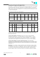
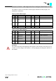
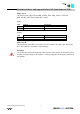
Structure of the in- and output data for LIGHTBUS (from firmware
WD)
Input
Content Description
Word High Low
n - Statusbyte Statusword
n+1 Input byte0 Input byte1 1. and 2. Input byte
n+2 - Input byte4 5.Input byte
n+3 Input byte3 Input byte2 3. and 4. Input byte
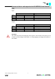
Output
Content Description
Word High Low
n - Statusbyte Statusword
n+1 Output byte0 Output byte1 1. and 2. Output byte
n+2 - Output byte4 5.Output byte
n+3 Output byte3 Output byte2 3. and 4. Output byte
Attention:
The control byte allows the changing of the registers of the module. It must always be 0
in order to avoid a change in the register. A wrong mapping can change the function of
the module!