UJA1167 Mini high-speed CAN system basis chip with Standby/Sleep modes & watchdog Rev. 2 — 18 April 2014 Product data sheet 1. General description The UJA1167 is a mini high-speed CAN System Basis Chip (SBC) containing an ISO 11898-2/5 compliant HS-CAN transceiver and an integrated 5 V/100 mA supply for a microcontroller. It also features a watchdog and a Serial Peripheral Interface (SPI).
UJA1167 NXP Semiconductors Mini high-speed CAN system basis chip with Standby/Sleep modes & watchdog Battery and CAN bus pins protected against automotive transients according to ISO 7637-3 Very low quiescent current in Standby and Sleep modes with full wake-up capability Leadless HVSON14 package (3.0 mm 4.5 mm) with improved Automated Optical Inspection (AOI) capability and low thermal resistance Dark green product (halogen free and Restriction of Hazardous Substances (RoHS) compliant) 2.
UJA1167 NXP Semiconductors Mini high-speed CAN system basis chip with Standby/Sleep modes & watchdog 2.6 Sensor supply voltage (pin VEXT of UJA1167TK/VX) 5 V nominal output; 2 % accuracy 30 mA output current capability Current limiting above 30 mA Excellent transient response with a 4.7 F ceramic output load capacitor Protected against short-circuits to GND and to the battery High ESD robustness of 6 kV according to IEC 61000-4-2 Can handle negative voltages as low as 18 V 3.
UJA1167 NXP Semiconductors Mini high-speed CAN system basis chip with Standby/Sleep modes & watchdog 4. Block diagram 8-$ %$7 +,*+ 92/7$*( 287387 ,1+ 9(;7 9 6(1625 6833/< 9 0,&52&21752//(5 6833/< 9 5671 9 :$7&+'2* 5;' 7;' :$.( 6&. 6', 6'2 6&61 +6 &$1 &$1+ &$1/ :$.( 83 63, *1' DDD (1) UJA1167TK only. (2) UJA1167TK/VX only. Fig 1.
UJA1167 NXP Semiconductors Mini high-speed CAN system basis chip with Standby/Sleep modes & watchdog 5. Pinning information 5.1 Pinning WHUPLQDO LQGH[ DUHD 7;' 6&61 *1' &$1+ 9 &$1/ 5;' 5671 %$7 6'2 :$.( ,1+ 9(;7 6&. 8-$ 6', DDD 7UDQVSDUHQW WRS YLHZ (1) INH in the UJA1167TK; VEXT in the UJA1167TK/VX Fig 2. Pin configuration diagram 5.2 Pin description Table 2.
UJA1167 NXP Semiconductors Mini high-speed CAN system basis chip with Standby/Sleep modes & watchdog 6. Functional description 6.1 System controller The system controller manages register configuration and controls the internal functions of the UJA1167. Detailed device status information is collected and made available to the microcontroller. 6.1.
UJA1167 NXP Semiconductors Mini high-speed CAN system basis chip with Standby/Sleep modes & watchdog NORMAL MC = Sleep & no wake-up pending & wake-up enabled & SLPC = 0 MC = Normal MC = Standby SLEEP STANDBY MC = Sleep & no wake-up pending & wake-up enabled & SLPC = 0 from Normal or Standby MC = Sleep & (wake-up pending OR wake-up disabled) any reset event RSTN = HIGH V1 undervoltage no overtemperature wake-up event RESET OVERTEMP power-on any reset event FORCED NORMAL VBAT undervoltage
UJA1167 NXP Semiconductors Mini high-speed CAN system basis chip with Standby/Sleep modes & watchdog Any enabled regular wake-up via CAN or WAKE or any diagnostic wake-up event will cause the UJA1167 to wake up from Sleep mode. The behavior of INH/VEXT is determined by the SPI settings. The SPI and the watchdog are disabled. Autonomous bus biasing is active. Sleep mode can be selected from Normal or Standby mode via an SPI command (MC = 001).
UJA1167 NXP Semiconductors Mini high-speed CAN system basis chip with Standby/Sleep modes & watchdog power-on detection threshold Vth(det)pon (triggering an initialization process) and switches to Reset mode after tstartup. In Off mode, the CAN pins disengage from the bus (zero load; high-ohmic). 6.1.1.6 Overtemp mode Overtemp mode is provided to prevent the UJA1167 being damaged by excessive temperatures.
UJA1167 NXP Semiconductors Mini high-speed CAN system basis chip with Standby/Sleep modes & watchdog The UJA1167 switches from Reset mode to Forced Normal mode if bit FNMC = 1. 6.1.1.8 Table 3.
UJA1167 NXP Semiconductors Mini high-speed CAN system basis chip with Standby/Sleep modes & watchdog Table 5.
UJA1167 NXP Semiconductors Mini high-speed CAN system basis chip with Standby/Sleep modes & watchdog A watchdog trigger event resets the watchdog timer. A watchdog trigger event is any valid write access to the Watchdog control register. If the watchdog mode or the watchdog period have changed as a result of the write access, the new values are immediately valid. Table 6.
UJA1167 NXP Semiconductors Mini high-speed CAN system basis chip with Standby/Sleep modes & watchdog Two operating modes have a major impact on the operation of the watchdog: Forced Normal mode and Software Development mode (Software Development mode is provided for test purposes and is not an SBC operating mode; the UJA1167 can be in any mode with Software Development mode enabled; see Section 6.2.1).
UJA1167 NXP Semiconductors Mini high-speed CAN system basis chip with Standby/Sleep modes & watchdog Table 9. Watchdog status register (address 05h) Bit Symbol Access Value Description 1:0 WDS R watchdog status: 00 watchdog is off 01 watchdog is in first half of window 10 watchdog is in second half of window 11 reserved 6.2.1 Software Development mode Software Development mode is provided to simplify the software design process.
UJA1167 NXP Semiconductors Mini high-speed CAN system basis chip with Standby/Sleep modes & watchdog When the SBC is in Sleep mode with watchdog Timeout mode selected, a wake-up event is generated after the nominal watchdog period (NWP). If bit WDF is set, RXD is forced LOW and V1 is turned on. The application software can then clear the WDF bit and trigger the watchdog before it overflows. 6.2.4 Watchdog behavior in Autonomous mode Autonomous mode is selected when WMC = 001.
UJA1167 NXP Semiconductors Mini high-speed CAN system basis chip with Standby/Sleep modes & watchdog 6.3.2 Selecting the output reset pulse width The duration of the output reset pulse is selected via bits RLC in the Start-up control register (Table 11). The SBC distinguishes between a cold start and a warm start.
UJA1167 NXP Semiconductors Mini high-speed CAN system basis chip with Standby/Sleep modes & watchdog 6.4 Global temperature protection The temperature of the UJA1167 is monitored continuously, except in Sleep and Off modes. The SBC switches to Overtemp mode if the temperature exceeds the overtemperature protection activation threshold, Tth(act)otp. In addition, pin RSTN is driven LOW and V1, VEXT and the CAN transceiver are switched off.
UJA1167 NXP Semiconductors Mini high-speed CAN system basis chip with Standby/Sleep modes & watchdog Table 12.
UJA1167 NXP Semiconductors Mini high-speed CAN system basis chip with Standby/Sleep modes & watchdog The default value of VEXTC at power-on is defined by bits VEXTSUC in non-volatile memory (see Section 6.11). In contrast to pin INH, pin VEXT is disabled when the SBC switches to Overtemp mode. The status of VEXT can be read from the Supply voltage status register (Table 13). 6.
UJA1167 NXP Semiconductors Mini high-speed CAN system basis chip with Standby/Sleep modes & watchdog The CAN transceiver is in Active mode when: • the UJA1167 is in Normal mode (MC = 111) and the CAN transceiver has been enabled by setting bits CMC in the CAN control register to 01 or 10 (see Table 14) and: – if CMC = 01, the voltage on pin V1 is above the 90 % undervoltage threshold – if CMC = 10, the voltage on pin V1 is above the V1 reset threshold If pin TXD is held LOW (e.g.
UJA1167 NXP Semiconductors Mini high-speed CAN system basis chip with Standby/Sleep modes & watchdog • the SBC switches to Reset or Standby or Sleep mode OR • the SBC is in Normal mode and CMC = 00 provided the CAN-bus has been inactive for at least tto(silence). If the CAN-bus has been inactive for less than tto(silence), the CAN transceiver switches first to CAN Offline Bias mode and then to CAN Offline mode once the bus has been silent for tto(silence).
UJA1167 NXP Semiconductors Mini high-speed CAN system basis chip with Standby/Sleep modes & watchdog &$1 $FWLYH >5HVHW 25 6WDQGE\ 25 6OHHS 25 1RUPDO &0& 25 &0& 9 9 25 &0& 99 9 57& @ W ! WWR VLOHQFH 1RUPDO > &0& 99 ! 25 &0& 99 ! 9 57& @ 1RUPDO > &0& 99 ! 25 &0& 99 ! 9 57& @ 1RUPDO &0& >5HVHW 25 6WDQGE\ 25 6OHHS 25 1RUPDO &0& 25 &0& 9 9 25 &0& 99 9 57& @ W WWR VLOHQF
UJA1167 NXP Semiconductors Mini high-speed CAN system basis chip with Standby/Sleep modes & watchdog dominant tdom ≥ twake(busdom) recessive dominant trec ≥ twake(busrec) tdom ≥ twake(busdom) twake < tto(wake) CAN wake-up 015aaa267 Fig 6. CAN wake-up timing When a valid CAN wake-up pattern is detected on the bus, wake-up bit CW in the Transceiver event status register is set (see Table 22) and pin RXD is driven LOW.
UJA1167 NXP Semiconductors Mini high-speed CAN system basis chip with Standby/Sleep modes & watchdog 6.8 CAN fail-safe features 6.8.1 TXD dominant timeout A TXD dominant time-out timer is started when pin TXD is forced LOW while the transceiver is in CAN Active Mode. If the LOW state on pin TXD persists for longer than the TXD dominant time-out time (tto(dom)TXD), the transmitter is disabled, releasing the bus lines to recessive state.
UJA1167 NXP Semiconductors Mini high-speed CAN system basis chip with Standby/Sleep modes & watchdog 6.10 Wake-up and interrupt event diagnosis via pin RXD Wake-up and interrupt event diagnosis in the UJA1167 is intended to provide the microcontroller with information on the status of a range of features and functions. This information is stored in the event status registers (Table 20 to Table 22) and is signaled on pin RXD, if enabled.
UJA1167 NXP Semiconductors Mini high-speed CAN system basis chip with Standby/Sleep modes & watchdog If an event occurs while the associated event capture function is enabled, the relevant event status bit is set. If the transceiver is in CAN Offline mode with V1 active (SBC Normal or Standby mode), pin RXD is forced LOW to indicate that a wake-up or interrupt event has been detected.
UJA1167 NXP Semiconductors Mini high-speed CAN system basis chip with Standby/Sleep modes & watchdog changes. At least one regular wake-up event must be enabled before the UJA1167 can switch to Sleep mode. Any attempt to enter Sleep mode while all regular wake-up events are disabled will trigger a system reset. Another condition that must be satisfied before the UJA1167 can switch to Sleep mode is that all event status bits must be cleared.
UJA1167 NXP Semiconductors Mini high-speed CAN system basis chip with Standby/Sleep modes & watchdog Table 21.
UJA1167 NXP Semiconductors Mini high-speed CAN system basis chip with Standby/Sleep modes & watchdog Table 25.
UJA1167 NXP Semiconductors Mini high-speed CAN system basis chip with Standby/Sleep modes & watchdog Table 28. Overview of MTPNV registers Address Register Name Bit: 7 6 5 4 3 2 0x73 Start-up control (see Table 11) reserved RLC VEXTSUC reserved 0x74 SBC configuration control (see Table 8) reserved V1RTSUC FNMC SDMC 1 0 reserved SLPC 6.11.
UJA1167 NXP Semiconductors Mini high-speed CAN system basis chip with Standby/Sleep modes & watchdog 6.11.1.1 Calculating the CRC value for MTP programming The cyclic redundancy check value stored in bits CRCC in the MTPNV CRC control register is calculated using the data written to registers 0x73 and 0x74. Table 30.
UJA1167 NXP Semiconductors Mini high-speed CAN system basis chip with Standby/Sleep modes & watchdog 6.11.2 Restoring factory preset values Factory preset values are restored if the following conditions apply for at least td(MTPNV) during power-up: • pin RSTN is held LOW • CANH is pulled up to VBAT • CANL is pulled down to GND After the factory preset values have been restored, the SBC performs a system reset and enters Forced normal Mode. Since the CAN bus is clamped dominant, pin RXDC is forced LOW.
UJA1167 NXP Semiconductors Mini high-speed CAN system basis chip with Standby/Sleep modes & watchdog Table 33.
UJA1167 NXP Semiconductors Mini high-speed CAN system basis chip with Standby/Sleep modes & watchdog SCSN SCK 01 02 03 04 N–1 N sampled SDI X SDO floating X MSB MSB–1 MSB–2 MSB–3 01 LSB MSB MSB–1 MSB–2 MSB–3 01 LSB X floating 015aaa255 Fig 8. SPI timing protocol The SPI data in the UJA1167 is stored in a number of dedicated 8-bit registers. Each register is assigned a unique 7-bit address. Two bytes must be transmitted to the SBC for a single register write operation.
UJA1167 NXP Semiconductors Mini high-speed CAN system basis chip with Standby/Sleep modes & watchdog During an SPI data read or write operation, the contents of the addressed register(s) is returned via pin SDO. The UJA1167 tolerates attempts to write to registers that don't exist. If the available address space is exceeded during a write operation, the data above the valid address range is ignored (without generating an SPI failure event).
UJA1167 NXP Semiconductors Mini high-speed CAN system basis chip with Standby/Sleep modes & watchdog 6.15.2 Register map The addressable register space contains 128 registers with addresses from 0x00 to 0x7F. An overview of the register mapping is provided in Table 34 to Table 42. The functionality of individual bits is discussed in more detail in relevant sections of the data sheet. Table 34.
UJA1167 NXP Semiconductors Mini high-speed CAN system basis chip with Standby/Sleep modes & watchdog Table 38. Address Overview of MTPNV status register Register Name Bit: 7 0x70 Table 39. Address MTPNV status 6 Table 40. Address Table 41. Address Register Name Table 42.
UJA1167 NXP Semiconductors Mini high-speed CAN system basis chip with Standby/Sleep modes & watchdog Table 43.
UJA1167 NXP Semiconductors Mini high-speed CAN system basis chip with Standby/Sleep modes & watchdog Table 43.
UJA1167 NXP Semiconductors Mini high-speed CAN system basis chip with Standby/Sleep modes & watchdog 7. Limiting values Table 44. Limiting values In accordance with the Absolute Maximum Rating System (IEC 60134). Symbol Parameter Conditions Vx voltage on pin x DC value voltage between pin CANH and pin CANL Vtrt transient voltage Max Unit V 0.2 +6 pins TXD, RXD, SDI, SDO, SCK, SCSN, RSTN 0.2 VV1 + 0.2 V pins INH/VEXT/WAKE 18 +40 V pin BAT 0.
UJA1167 NXP Semiconductors Mini high-speed CAN system basis chip with Standby/Sleep modes & watchdog 8. Thermal characteristics Table 45. Symbol Rth(vj-a) [1] Thermal characteristics Parameter Conditions [1] thermal resistance from virtual junction to ambient HVSON14 Typ Unit 60 K/W According to JEDEC JESD51-2, JESD51-5 and JESD51-7 at natural convection on 2s2p board.
UJA1167 NXP Semiconductors Mini high-speed CAN system basis chip with Standby/Sleep modes & watchdog Table 46. Static characteristics …continued Tvj = 40 C to +150 C; VBAT = 3 V to 28 V; R(CANH-CANL) = 60 ; all voltages are defined with respect to ground; positive currents flow into the IC; typical values are given at VBAT = 13 V; unless otherwise specified. Symbol Parameter Conditions Min Typ Max Unit VBAT = 5.5 V to 18 V; IV1 = 120 mA to 0 mA; VTXD = VV1 4.9 5 5.1 V VBAT = 5.
UJA1167 NXP Semiconductors Mini high-speed CAN system basis chip with Standby/Sleep modes & watchdog Table 46. Static characteristics …continued Tvj = 40 C to +150 C; VBAT = 3 V to 28 V; R(CANH-CANL) = 60 ; all voltages are defined with respect to ground; positive currents flow into the IC; typical values are given at VBAT = 13 V; unless otherwise specified.
UJA1167 NXP Semiconductors Mini high-speed CAN system basis chip with Standby/Sleep modes & watchdog Table 46. Static characteristics …continued Tvj = 40 C to +150 C; VBAT = 3 V to 28 V; R(CANH-CANL) = 60 ; all voltages are defined with respect to ground; positive currents flow into the IC; typical values are given at VBAT = 13 V; unless otherwise specified.
UJA1167 NXP Semiconductors Mini high-speed CAN system basis chip with Standby/Sleep modes & watchdog 10. Dynamic characteristics Table 47. Dynamic characteristics Tvj = 40 C to +150 C; VBAT = 3 V to 28 V; R(CANH-CANL) = 60 ; all voltages are defined with respect to ground; positive currents flow into the IC; typical values are given at VBAT = 13 V; unless otherwise specified.
UJA1167 NXP Semiconductors Mini high-speed CAN system basis chip with Standby/Sleep modes & watchdog Table 47. Dynamic characteristics …continued Tvj = 40 C to +150 C; VBAT = 3 V to 28 V; R(CANH-CANL) = 60 ; all voltages are defined with respect to ground; positive currents flow into the IC; typical values are given at VBAT = 13 V; unless otherwise specified.
UJA1167 NXP Semiconductors Mini high-speed CAN system basis chip with Standby/Sleep modes & watchdog Table 47. Dynamic characteristics …continued Tvj = 40 C to +150 C; VBAT = 3 V to 28 V; R(CANH-CANL) = 60 ; all voltages are defined with respect to ground; positive currents flow into the IC; typical values are given at VBAT = 13 V; unless otherwise specified. Symbol Parameter Conditions Min Typ Max Unit 50 - - s 0.9 - 1.
UJA1167 NXP Semiconductors Mini high-speed CAN system basis chip with Standby/Sleep modes & watchdog 7;' [ WELW 7;' WELW 7;' 5;' WELW 5;' DDD Fig 11. Loop delay symmetry timing diagram 6&61 W63,/($' W63,/$* WF\ FON WFON + WFON / WVX ' WK ' W:+ 6 6&. 6', 06% ; /6% ; WY 4 IORDWLQJ 6'2 IORDWLQJ ; 06% /6% DDD Fig 12. SPI timing diagram UJA1167 Product data sheet All information provided in this document is subject to legal disclaimers. Rev.
UJA1167 NXP Semiconductors Mini high-speed CAN system basis chip with Standby/Sleep modes & watchdog 11. Application information 11.1 Application diagram H J RII ERDUG VHQVRU VXSSO\ %$7 ) %$7 Nȍ :$.( 9 9(;7 5671 Q) 8-$ 7. 9; *1' 5671 &$1+ 57 9&& 0,&52 &21752//(5 6&61 6'2 VWDQGDUG & SRUWV 6&. 6', 5;' 7;' 5;' 7;' 966 &$1/ 57 H J Q) DDD (1) Actual capacitance value must be a least 1.
UJA1167 NXP Semiconductors Mini high-speed CAN system basis chip with Standby/Sleep modes & watchdog H J ,1+ DV FRQWURO VLJQDO IRU YROWDJH UHJXODWRU 9 %$7 ) 9 ,1+ %$7 ,1+ Nȍ 9 :$.( 5671 5671 Q) 8-$ 7. *1' &$1+ 57 9&& 0,&52 &21752//(5 6&61 6'2 VWDQGDUG & SRUWV 6&. 6', 5;' 7;' 5;' 7;' 966 &$1/ 57 H J Q) DDD (1) Actual capacitance value must be a least 1.
UJA1167 NXP Semiconductors Mini high-speed CAN system basis chip with Standby/Sleep modes & watchdog 12. Test information BAT RXD CANH RL SBC 15 pF TXD 100 pF CANL GND 015aaa369 Fig 15. Timing test circuit for CAN transceiver 10 1 BAT TXD CANH 13 30 Ω f = 250 kHz CSPLIT 4.7 nF SBC 4 RXD CANL 30 Ω 12 GND 2 015aaa444 Fig 16. Test circuit for measuring transceiver driver symmetry 12.
UJA1167 NXP Semiconductors Mini high-speed CAN system basis chip with Standby/Sleep modes & watchdog 13.
UJA1167 NXP Semiconductors Mini high-speed CAN system basis chip with Standby/Sleep modes & watchdog 14. Handling information All input and output pins are protected against ElectroStatic Discharge (ESD) under normal handling. When handling ensure that the appropriate precautions are taken as described in JESD625-A or equivalent standards. 15. Soldering of SMD packages This text provides a very brief insight into a complex technology.
UJA1167 NXP Semiconductors Mini high-speed CAN system basis chip with Standby/Sleep modes & watchdog • Process issues, such as application of adhesive and flux, clinching of leads, board transport, the solder wave parameters, and the time during which components are exposed to the wave • Solder bath specifications, including temperature and impurities 15.
UJA1167 NXP Semiconductors Mini high-speed CAN system basis chip with Standby/Sleep modes & watchdog maximum peak temperature = MSL limit, damage level temperature minimum peak temperature = minimum soldering temperature peak temperature time 001aac844 MSL: Moisture Sensitivity Level Fig 18. Temperature profiles for large and small components For further information on temperature profiles, refer to Application Note AN10365 “Surface mount reflow soldering description”. 16.
UJA1167 NXP Semiconductors Mini high-speed CAN system basis chip with Standby/Sleep modes & watchdog 17. Revision history Table 50. Revision history Document ID Release date Data sheet status Change notice Supersedes UJA1167 v.2 20140418 Product data sheet - UJA1167 v.1 Modifications: • • • • • • • • • • • • • • • • • • • UJA1167 v.1 UJA1167 Product data sheet Section 1: text revised (2nd paragraph added) Section 2.
UJA1167 NXP Semiconductors Mini high-speed CAN system basis chip with Standby/Sleep modes & watchdog 18. Legal information 18.1 Data sheet status Document status[1][2] Product status[3] Definition Objective [short] data sheet Development This document contains data from the objective specification for product development. Preliminary [short] data sheet Qualification This document contains data from the preliminary specification.
UJA1167 NXP Semiconductors Mini high-speed CAN system basis chip with Standby/Sleep modes & watchdog No offer to sell or license — Nothing in this document may be interpreted or construed as an offer to sell products that is open for acceptance or the grant, conveyance or implication of any license under any copyrights, patents or other industrial or intellectual property rights. Translations — A non-English (translated) version of a document is for reference only.
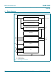
UJA1167 NXP Semiconductors Mini high-speed CAN system basis chip with Standby/Sleep modes & watchdog 20. Contents 1 2 2.1 2.2 2.3 2.4 2.5 2.6 3 4 5 5.1 5.2 6 6.1 6.1.1 6.1.1.1 6.1.1.2 6.1.1.3 6.1.1.4 6.1.1.5 6.1.1.6 6.1.1.7 6.1.1.8 6.1.2 6.2 6.2.1 6.2.2 6.2.3 6.2.4 6.3 6.3.1 6.3.2 6.3.3 6.4 6.5 6.5.1 6.5.2 6.6 6.7 6.7.1 6.7.1.1 General description . . . . . . . . . . . . . . . . . . . . . . 1 Features and benefits . . . . . . . . . . . . . . . . . . . . 1 General . . . . . . . . . . . . . . . . . . . .
UJA1167 NXP Semiconductors Mini high-speed CAN system basis chip with Standby/Sleep modes & watchdog 17 18 18.1 18.2 18.3 18.4 19 20 Revision history . . . . . . . . . . . . . . . . . . . . . . . . Legal information. . . . . . . . . . . . . . . . . . . . . . . Data sheet status . . . . . . . . . . . . . . . . . . . . . . Definitions . . . . . . . . . . . . . . . . . . . . . . . . . . . . Disclaimers . . . . . . . . . . . . . . . . . . . . . . . . . . . Trademarks. . . . . . . . . . . . . . . . . . . . .