
Product Specifications
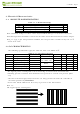
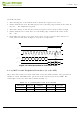

In the Read mode:
1. After dri
ving CS# to low, MCU need to define the register to be read.
2. SDA is shifted into an 8-bit shift register on each rising edge of SCL in the order of
D7, D6, ... D0 with D/C# keep low.
3. After SCL change to low for the last bit of register, D/C# need to drive to high.
4. SDA is shifted out an 8-bit data on each falling edge of SCL in the order of D7,
D6, … D0.
5. Depending on register type, more than 1 byte can be read out. After all byte are
read, CS# need to drive to high to stop the read operation
.
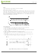
3.5-3) MCU Serial P
eripheral Interface (3-wire SPI)
The 3-wire SPI consists o
f serial clock SCL, serial data SDA and CS#. The operation is
similar to 4-wire SPI while
D/C# pin is not used and
it must be tied to LOW. The
control pins status in 3-wire SPI is shown in Table 7-3.
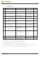
Table 3.5-3 : Contro
l pins status of 3-wire SPI
Function SCL pin SDA pin D/C# pin CS# pin
Write
↑
Command bit Tie LOW
L
W
ri
te da
t
a
↑
Da
t
a bi
t Ti
e L
O
W
L
Figure v-2: Read procedure in 4-wire SPI mode
2.13inch e-Paper
www.waveshare.com
15/39