
Product Specifications
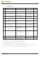

Note:
(1)L is connected to V
SS
and H is connected to V
DDIO
(2)↑ stands for rising edge of signal
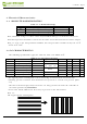
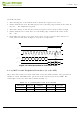
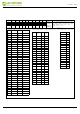
In the write operation, a 9-bit data will be shifted into the shift register on each clock
rising edge. The bit shifting sequence is D/C# bit, D7 bit, D6 bit to D0 bit. The first
bit is D/C# bit which determines the following byte is command or data. When D/C#
bit is 0, the following byte is command. When D/C# bit is 1, the following byte is data.
shows the write procedure in 3-wire SPI
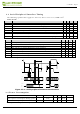
1. After driving CS# to
low, MCU need to define the register to be read.
2. D/C#=0 is shifted thru SDA with one rising edge of SCL
3. SDA is shifted into an 8-bit shift register on each rising edge of SCL in the order of
D7, D6, ... D0.
4. D/C#=1 is shifted thru SDA with one rising edge of SCL
5. SDA is shifted out an 8-bit data on each falling edge of SCL in the order of D7,
D6, … D0.
6. Depending on register type, more than 1 byte can be read out. After all byte are
read, CS# need to drive to high to stop the read operation.
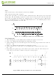
Figure 3.5-3: Read procedure in 3-wire SPI mode
S#
SCL
C
SDA
(Write
Mode)
Figure 3.5-3: Write proced
ure in 3-wire SPI mode
0 D7 D6 D5 D4 D3 D2 D1 D0 1 D7
In the Read mode:
2.13inch e-Paper
www.waveshare.com
16/39