
Product Specifications
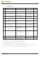
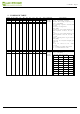
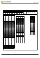

5. COMMAND TABLE
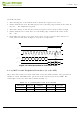
R/W# D/C# Hex D7 D6 D5 D4 D3 D2 D1 D0 Command
Description
0
0
01 01
0
0
0
0
0
0
1
Driver
Output
control
Gate setting
A[8
:0]= 127h [POR], 296 MUX
MUX Gate line
s setting as (A[8:0] + 1).
B[2:0] = 000 [POR].
Gate scanning
sequence and direction
B[2]: GD
Selects the 1st ou
tput Gate
GD=0 [POR],
G0 is the 1st g
ate output channel, gate
output sequenc
e is G0,G1, G2, G3, …
GD=1,
G1 is the 1st gate
output channel, gate
output sequenc
e is G1, G0, G3, G2, …
B[1]: SM
Change scanning orde
r of gate driver.
S
M=0 [POR],
G0, G1, G2, G
3…295 (left and right gate
interlaced)
SM=1,
G0, G2, G4 …G294, G1,
G3, …G295
B[0]: TB
TB = 0 [POR], scan
from G0 to G295
TB = 1, scan from G
295 to G0.
0
1
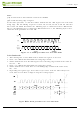
A7 A6 A5 A4 A3 A2 A1 A0
0
1
0
0
0
0
0
0
0
A8
0
1
0
0
0
0
0
B2 B1 B0
0
0
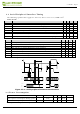
03
0
0
0
0
0
0
1
1
Gate
Driving
voltage
Control
Set Gate dri
ving voltage
A[4:0] = 00h [POR]
VGH setting from 1
2V to
20V
0
1
0
0
0
A4 A3 A2 A1 A0
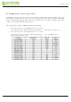
A[4:0] VGH A[4:0] VGH
07h 12 10h 16.5
08h 12.5 11h 17
09h 13 12h 17.5
0Ah 13.5 13h 18
0
B
h 14 1
4h 18.
5
0Ch 14.5 15h 19
0Dh 15 16h 19.5
0Eh 15.5 17h 20
0Fh 16 Other NA
2.13inch e-Paper
www.waveshare.com
19/39