
Product Specifications
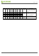
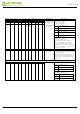
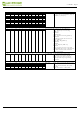

R/W# D/C# Hex D7 D6 D5 D4 D3 D2 D1 D0 Command
Description
0
0
24
0
0
1
0
0
1
0
0
Write RAM
(BW)
After this com
mand, data entries will
bewritten into the
BW RAM until
an
o
t
h
e
r
c
o
m
m
a
n
d
is written. Address
pointers
willadvance accordi
ngly
For Write pixel:
Content of Write RAM(BW) = 1
For
Black pixel:
Conten
t of Write RAM(BW) = 0
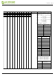
0
0
26
0
0
1
0
0
1
1
0
Write RAM
(RED)
After this co
mmand, data entries will
bewritten into the
RED RAM until
an
othercommand
is written. Address
pointers
w
illa
d
v
a
n
c
e a
c
c
o
r
di
ngly.
For Red pixel:
Content of Write RAM(RED) = 1
For non-Red pixel [
Black or White]:
Content of Write RAM(RED) = 0
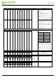
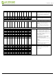
0
0
27
0
0
1
0
0
1
1
1
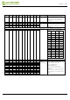
Read RAM After this
command, data read on the
MCU bus will fetc
h data from RAM
[According to parameter
of Register
41h to select reading RAM(BW) /
RAM(RED)], until anot
her command is
written.
Address pointers will advance
accordingly.
The
1st byte of data read is dummy
dat
a.
0
0
28
0
0
1
0
1
0
0
0
VCOM Sense Enter VC
OM sensing conditions and
holdfor
d
u
r
a
t
io
n
d
e
f
in
e
d
in 29h before
readingVCOM value.
The sensed VCOM
voltage is stored
in
register
The command req
uired CLKEN=1
and
ANALOGEN=1
Refer to Regist
er 0x22 for detail.
BUSY pad
will output high during
o
peration.
0
0
29
0
0
1
0
1
0
0
1
VCOM Sense
Duration
Stabling t
ime between entering
VCOMsensing mo
de and reading
acquired.
A[3:0] = 09h [POR],
d
uration = 10s.
VCOM sense duration = (A[3:0]+1)
sec
0
1
0
1
0
0
A3 A2 A1 A0
2.13inch e-Paper
www.waveshare.com
27/39