
Product Specifications

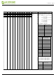
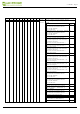
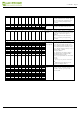

R/W# D/C# Hex D7 D6 D5 D4 D3 D2 D1 D0 Command
Description
0
0
2A
0
0
1
0
1
0
1
0
Program VCOM
OTP
Program VCOM reg
ister into OTP
The command requ
ired
CLKEN=1.
Refer to Register
0x22 for detail.
BUSY pad will out
put high during
operation.
0
0
2B
0
0
1
0
1
0
1
1
Write Register
for
VCOM Control
This command is used
to reduce
glitch
when ACVCOM toggle
. Two data bytes
D04h and D63h should b
e set for this
command.
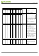
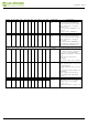
0
1
0
0
0
0
0
1
0
0
0
1
0
1
1
0
0
0
1
1
0
0
2C
0
0
1
0
1
1
0
0
Write VCOM
register
Write VCOM re
gister from MCU
interface
A[7:0] = 00h [POR]
A[7:0]
VCOM
A[7:0]
VCOM
08h
-0.2 44h
-1.7
0Ch
-0.3 48h
-1.8
10h
-0.4 4Ch
-1.9
14h
-0.5 50h
-2
18h
-0.6 54h
-2.1
1Ch
-0.7 58h
-2.2
20h
-0.8 5Ch
-2.3
24h
-0.9 60h
-2.4
28h
-1 64h
-2.5
2Ch
-1.1 68h
-2.6
30h
-1.2 6Ch
-2.7
34h
-1.3 70h
-2.8
38h
-1.4 74h
-2.9
3Ch
-1.5 78h
-3
40h
-1.6 Ot
h
e
r
NA
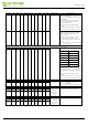
0
1
A7 A6 A5 A4 A3 A2 A1 A0
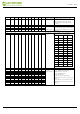
0
0
2D
0
0
1
0
1
1
0
1
OTP Register
Read for
Display Option
Read R
egister for Display Option:
A[7:0]: VCOM OTP Sele
ction
(Command 0x37,
Byte A)
B[7:0]: VCOM Register
(
C
o
m
m
a
n
d 0x
2C
)
C
[7
:0
]~
F
[7:0]: Display Mode
(Command 0x37,
Byte B to Byte G)
[5 bytes]
G[7:0]~H[7:0]: Waveform Version
(Command 0x37, B
yte H to Byte K)
[4 bytes]
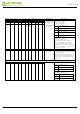
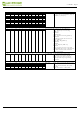
1
1
A7 A6 A5 A4 A3 A2 A1 A0
1
1
B7 B6 B5 B4 B3 B2 B1 B0
1
1
C7 C6 C5 C4 C3 C2 C1 C0
1
1
D7 D6 D5 D4 D3 D2 D1 D0
1
1
E7 E6 E5 E4 E3 E2 E1 E0
1
1
F7 F6 F5 F4 F3 F2 F1 F0
1
1
G7 G6 G5 G4 G3 G2 G1 G0
1
1
H7 H6 H5 H4 H3 H2 H1 H0
1
1
I7 I6 I5 I4 I3 I2 I1 I0
1
1
J7 J6 J5 J4 J3 J2 J1 J0
1
1
K7 K6 K5 K4 K3 K2 K1 K0
2.13inch e-Paper
www.waveshare.com
28/39