
Product Specifications
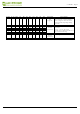
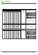
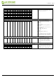

R/W# D/C# Hex D7 D6 D5 D4 D3 D2 D1 D0 Command
Description
0
0
34
0
0
1
1
0
1
0
0
CRC calculation CRC c
alculation command for OTP
content validation
. For details, please
refer
to SSD1675B applic
ation note.
BUSY pad will output high during
operation.
0
0
35
0
0
1
1
0
1
0
1
CRC Status
Read
CRC Status Read
A[15
:0] is the CRC read out value
1
1 A15 A14 A13 A12 A11 A10 A9 A
8
1
1
A7 A6 A5 A4 A3 A2 A1 A0
0
0
36
0
0
1
1
0
1
1
0
Program OTP
selection
Program OTP Selection according to
the
OTP Selection Control [R37h and
R38h]
The command requir
ed
CLKEN=1.
Refer to Register 0x22 for detail.
BUSY pad will out
put high during
operation.
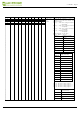
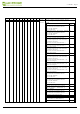
0
1
37
0
0
1
1
0
1
1
1
Write Register
for
Display Option
Write R
egister for Display Option
B[7:0] Display Mod
e for WS[7:0]
C
[7
:0
]
D
i
s
p
l
a
y
M
o
d
e for WS[15:8]
D[7:0] Display Mod
e for WS[23:16]
E[7:0] Display Mod
e for WS[31:24]
F[3:0] Display Mode
for WS[35:32]
0:
Display Mode 1 [PO
R]
1: Display Mode2
F[6]: PingPong for Display Mode 2
0: RAM ping-pong disable [P
OR]
1: RAM ping-pong enable
G
[7:0]~J[7:0] module ID /waveform
version.
Remarks:
1)
A[7:0]~J[7:0] can be s
tored in
OTP
2)
RAM ping-pong functio
n is not
support
for Display Mode 1
0
1
0
0
0
0
0
0
0
0
0
1
B7 B6 B5 B4 B3 B2 B1 B0
0
1
C7 C6 C5 C4 C3 C2 C1 C0
0
1
D7 D6 D5 D4 D3 D2 D1 D0
0
1
E7 E6 E5 E4 E3 E2 E1 E0
0
1
F7 F6 F5 F4 F3 F2 F1 F0
0
1
G7 G6 G5 G4 G3 G2 G1 G0
0
1
H7 H6 H5 H4 H3 H2 H1 H0
0
1
I7 I6 I5 I4 I3 I2 I1 I0
0
1
J7 J6 J5 J4 J3 J2 J1 J0
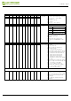
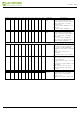
0
0
38
0
0
1
1
1
0
0
0
Write Register
for User
ID
Write Registe
r for User ID
A[7:0]]~J[7:0]: UserID
[10 bytes]
Remarks: A[7:0]~J[7
:0] can be
stored in
OTP
0
1
A7 A6 A5 A4 A3 A2 A1 A0
0
1
B7 B6 B5 B4 B3 B2 B1 B0
0
1
C7 C6 C5 C4 C3 C2 C1 C0
0
1
D7 D6 D5 D4 D3 D2 D1 D0
0
1
E7 E6 E5 E4 E3 E2 E1 E0
0
1
F7 F6 F5 F4 F3 F2 F1 F0
0
1
G7 G6 G5 G4 G3 G2 G1 G0
0
1
H7 H6 H5 H4 H3 H2 H1 H0
0
1
I7 I6 I5 I4 I3 I2 I1 I0
0
1
J7 J6 J5 J4 J3 J2 J1 J0
2.13inch e-Paper
www.waveshare.com
30/39