
Specification
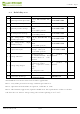
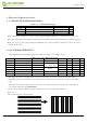


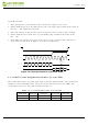
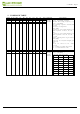
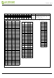
Table Of Contents

3.3 Serial Periphe
ral Interface Timing
The following specif
ications apply for: VSS=0V, VCI=2.2V to 3.7V, T
OPR
=25℃
Write mode
Symbol Parameter Min Typ
Max Unit
fSCL SCL frequency (W
rite Mode) 20 MHz
tCSSU Time CS# has to be low before t
he first rising edge of SCLK 20 ns
tCSHLD Time CS# has to remain low
after the last falling edge of SCLK 20 ns
tCSHIGH Time CS# has to
remain high between two transfers 100 ns
tSCLHIGH Part of the clo
ck period where SCL has to remain high 25 ns
tSCLLOW Part of the clock perio
d where SCL has to remain low 25 ns
tSISU Time SI (SDA Write Mode) ha
s to be stable before the next rising edge of SCL 10 ns
tSIHLD Time SI (SDA Write Mode) ha
s to remain stable after the rising edge of SCL 40 ns
Read mode
Symbol Parameter Min Typ Max Unit
f
SC
L S
C
L
f
r
e
qu
e
n
c
y
(
Read Mode) 2.5 MHz
tCSSU Time CS# has to be low befor
e the first rising edge of SCLK 100 ns
tCSHLD Time CS# has to remain low
after the last falling edge of SCLK 50 ns
tCSHIGH Time CS# has to
remain high between two transfers 250 ns
tSCLHIG Part of the clock pe
riod where SCL has to remain high 180 ns
tSCLLOW Part of the clock perio
d where SCL has to remain low 180 ns
tSOSU Time SO(SDA Read Mode
) will be stable before the next rising edge of SCL 50 ns
tSOHLD Time SO (SDA Read Mode) w
ill remain stable after the falling edge of SCL 0 ns
N
o
t
e: Al
l t
i
m
i
n
g
s a
re b
as
e
d on 2
0% to 80% of VDDIO-VSS
Parameter Symbol Conditions TYP Max Unit Remark
Panel power consum
ption during update -
25℃
- 18 mAs -
Deep sleep mode -
25℃
- 2 uA -
mAs=update average cur
rent×update time
Figure 3.3-1 : Serial peripheral interface characteristics
3.4 Power Consumption
2.13inch e-Paper
www.waveshare.com
13/39