
Specification

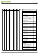

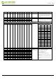
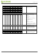
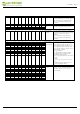
Table Of Contents

R/W#
D/C#
Hex
D7
D6
D5
D4
D3
D2 D1
D0
Command
Description
0
0
2E
0
0
1
0
1
1
1
0
User ID Read Read 10
Byte User ID stored in OTP:
A[7:0]]~J[7:0]: UserID (R38, Byte A
and Byte J) [10 bytes]
1
1
A7 A6 A5 A4 A3 A2 A1 A0
1
1
B7 B6 B5 B4 B3 B2 B1 B0
1
1
C7 C6 C5 C4 C3 C2 C1 C0
1
1
D7 D6 D5 D4 D3 D2 D1 D0
1
1
E7 E6 E5 E4 E3 E2 E1 E0
1
1
F7 F6 F5 F4 F3 F2 F1 F0
1
1
G
7 G
6 G
5 G
4 G
3 G
2 G
1 G
0
1
1
H7 H6 H5 H4 H3 H2 H1 H0
1
1
I7 I6 I5 I4 I3 I2 I1 I0
1
1
J7 J6 J5 J4 J3 J2 J1 J0
0
0
2F
0
0
1
0
1
1
1
1
Status Bit Read Read IC status Bit [POR 0x01]
A[5]: HV Ready Detection flag
[POR=0]
0: Ready
1: Not Ready
A[4]: V
CI Detection flag [POR=0]
0: Normal
1: VCI lower t
han the Detect level
A[3]: [POR=0]
A[2]: Bus
y flag [POR=0]
0: Normal
1: BUSY
A[1:0]: Chip
ID [POR=01]
Remark:
A[5] and A[4] status are not valid
after
RESET, they ne
ed to be initiated
by
command 0x14 a
nd command
0x15
respectively.
1
1
0
0
A5 A4
0
A2 A1 A0
0
0
31
0
0
1
1
0
0
0
1
L
o
a
d
W
S O
TP Lo
ad
O
T
P
o
f
Waveform Setting
The command req
uired
CLKEN=1.
Refer to Regist
er 0x22 for detail.
BUSY pad will ou
tput high during
operation.
0
0
32
0
0
1
1
0
0
1
0
Write LUT
register
Write LUT r
egister from MCU interface
[100 bytes], whi
ch contains the
content of
VS [nX-LUT], TP #[nX
],
RP#[n]).
Refer to Sess
ion 6.7 Waveform
0
1
A7 A6 A5 A4 A3 A2 A1 A0
0
1
B7 B6 B5 B4 B3 B2 B1 B0
0
1
:
:
:
:
:
:
:
:
0
1
.
..
.
.
.
.
.
.
2.13inch e-Paper
www.waveshare.com
29/39