
Data Sheet


www.waveshare.com
6/40
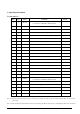
Pin #
Type
Single
Description
Remark
1
I
MFCSB
Serial communication chip select.
It would bypass to MFCSB by R61H command.
2
O
GDR
N-Channel MOSFET Gate Drive Control
3
O
RESE
Current Sense Input for the Control Loop
4
C
VGL
Negative Gate driving voltage
5
C
VGH
Positive Gate driving voltage
6
O
TSCL
I2C Interface to digital temperature sensor Clock pin
7
I/O
TSDA
I2C Interface to digital temperature sensor Date pin
8
I
BS1
Bus selection pin
Note 5-5
9
O
BUSY
Busy state output pin
Note 5-4
10
I
RES #
Reset
Note 5-3
11
I
D/C #
Data /Command control pin
Note 5-2
12
I
CS #
Chip Select input pin
Note 5-1
13
I/O
D0
serial clock pin (SPI)
14
I/O
D1
serial data pin (SPI)
15
I
VDDIO
Power for interface logic pins
16
I
VCI
Power Supply pin for the chip
17
VSS
Ground
18
C
VDD
Core logic power pin
19
O
FMSDO
Serial communication data output.
It would bypass to FMSDO by R61H command.
20
C
VSH
Positive Source driving voltage
21
C
PREVGH
Power Supply pin for VGH and VSH
22
C
VSL
Negative Source driving voltage
23
C
PREVGL
Power Supply pin for VCOM, VGL and VSL
24
C
VCOM
VCOM driving voltage
5.
Input/Output Terminals
5-1) Pin out List
Note 5-1: This pin (CS#) is the chip select input connecting to the MCU. The chip is enabled for MCU communication only when CS# is
pulled Low.
Note 5-2: This pin (D/C#) is Data/Command control pin connecting to the MCU. When the pin is pulled High, the data will be interpreted