SN65HVD230 SN65HVD231 SN65HVD232 SLOS346G – MARCH 2001 – REVISED JUNE 2002 3.3-V CAN TRANSCEIVERS FEATURES D Operates With a 3.
SN65HVD230 SN65HVD231 SN65HVD232 SLOS346G – MARCH 2001 – REVISED JUNE 2002 DESCRIPTION The SN65HVD230, SN65HVD231, and SN65HVD232 controller area network (CAN) transceivers are designed for use with the Texas Instruments TMS320Lx240x 3.3-V DSPs with CAN controllers, or with equivalent devices. They are intended for use in applications employing the CAN serial communication physical layer in accordance with the ISO 11898 standard.
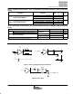
SN65HVD230 SN65HVD231 SN65HVD232 SLOS346G – MARCH 2001 – REVISED JUNE 2002 Function Tables DRIVER (SN65HVD230, SN65HVD231) OUTPUTS INPUT D RS CANH L CANL BUS STATE H L Dominant H V(Rs) < 1.2 12V Z Z Recessive Open X Z Z Recessive X V(Rs) > 0.
SN65HVD230 SN65HVD231 SN65HVD232 SLOS346G – MARCH 2001 – REVISED JUNE 2002 Function Tables (Continued) TRANSCEIVER MODES (SN65HVD230, SN65HVD231) V(Rs) V(Rs) > 0.75 VCC OPERATING MODE 10 kΩ to 100 kΩ to ground Slope control V(Rs) < 1 V High speed (no slope control) Standby Terminal Functions SN65HVD230, SN65HVD231 TERMINAL NAME DESCRIPTION NO.
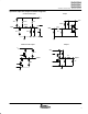
SN65HVD230 SN65HVD231 SN65HVD232 SLOS346G – MARCH 2001 – REVISED JUNE 2002 equivalent input and output schematic diagrams CANH and CANL Inputs D Input VCC VCC 110 kΩ 16 V 9 kΩ 100 kΩ 45 kΩ Input 1 kΩ Input 20 V 9 kΩ 9V CANH and CANL Outputs R Output VCC VCC 16 V 5Ω Output Output 9V 20 V www.ti.
SN65HVD230 SN65HVD231 SN65HVD232 SLOS346G – MARCH 2001 – REVISED JUNE 2002 absolute maximum ratings over operating free-air temperature (see Note 1) (unless otherwise noted)† Supply voltage range, VCC . . . . . . . . . . . . . . . . . . . . . . . . . . . . . . . . . . . . . . . . . . . . . . . . . . . . . . . . . . . . . . . – 0.3 V to 6 V Voltage range at any bus terminal (CANH or CANL) . . . . . . . . . . . . . . . . . . . . . . . . . . . . . . . . . . . . . . . . . .
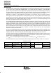
SN65HVD230 SN65HVD231 SN65HVD232 SLOS346G – MARCH 2001 – REVISED JUNE 2002 driver electrical characteristics over recommended operating conditions (unless otherwise noted) PARAMETER VOH TEST CONDITIONS VOD(D) VOD(R) VI = 0 V, See Figure 1 and Figure 3 CANH Recessive VI = 3 V, See Figure 1 and Figure 3 See Figure 1 1.5 2 3 Dominant VI = 0 V, VI = 0 V, See Figure 2 1.2 2 3 VI = 3 V, VI = 3 V, See Figure 1 – 120 0 12 Recessive No load – 0.5 – 0.2 0.
SN65HVD230 SN65HVD231 SN65HVD232 SLOS346G – MARCH 2001 – REVISED JUNE 2002 driver switching characteristics over recommended operating conditions(unless otherwise noted) SN65HVD232 PARAMETER TEST CONDITIONS MIN TYP MAX 35 85 UNIT ns 70 120 ns tPLH tPHL Propagation delay time, low-to-high-level output tsk(p) tr Pulse skew (|tP(HL) – tP(LH)|) Differential output signal rise time 25 50 100 ns tf Differential output signal fall time 40 55 80 ns Propagation delay time, high-to-low-level
SN65HVD230 SN65HVD231 SN65HVD232 SLOS346G – MARCH 2001 – REVISED JUNE 2002 device switching characteristics over recommended operating conditions (unless otherwise noted) TEST CONDITIONS PARAMETER t(LOOP1) t(LOOP2) Total loop delay, driver input to receiver output recessive to dominant output, Total loop delay, driver input to receiver output, output dominant to recessive MIN TYP MAX V(Rs) = 0 V, RS with 10 kΩ to ground, See Figure 9 70 115 See Figure 9 105 175 RS with 100 kΩ to ground, Se
SN65HVD230 SN65HVD231 SN65HVD232 SLOS346G – MARCH 2001 – REVISED JUNE 2002 PARAMETER MEASUREMENT INFORMATION Dominant CANH Recessive CANL ≈3V VOH ≈ 2.3 V VOL ≈1V VOH CANH CANL Figure 3. Driver Output Voltage Definitions RL = 60 Ω Signal Generator (see Note A) CL = 50 pF VO (see Note B) 50 Ω RS = 0 Ω to 100 kΩ for SN65HVD230 and SN65HVD231 N/A for SN65HVD232 3V Input 1.5 V 0V tPLH tPHL VOD(D) 90% 0.9 V Output 0.5 V 10% VOD(R) tr tf NOTES: A.
SN65HVD230 SN65HVD231 SN65HVD232 SLOS346G – MARCH 2001 – REVISED JUNE 2002 PARAMETER MEASUREMENT INFORMATION Output Signal Generator (see Note A) 50 Ω 1.5 V CL = 15 pF (see Note B) 2.9 V Input 2.2 V 1.5 V tPLH tPHL VOH 90% Output 1.3 V 10% VOL tr tf NOTES: A. The input pulse is supplied by a generator having the following characteristics: PRR ≤ 500 kHz, 50% duty cycle, tr ≤ 6 ns, tf ≤ 6 ns, Zo = 50 Ω. B. CL includes probe and jig capacitance. Figure 6.
SN65HVD230 SN65HVD231 SN65HVD232 SLOS346G – MARCH 2001 – REVISED JUNE 2002 PARAMETER MEASUREMENT INFORMATION Table 1. Receiver Characteristics Over Common Mode With V(Rs) = 1.2 V VIC –2 V VID 900 mV VCANH –1.55 V VCANL –2.45 V R OUTPUT 7V 900 mV 8.45 V 6.55 V L 1V 6V 4V –2 V L L 4V 6V 7V 1V L –2 V 500 mV –1.75 V –2.25 V H 7V 500 mV 7.25 V 6.
SN65HVD230 SN65HVD231 SN65HVD232 SLOS346G – MARCH 2001 – REVISED JUNE 2002 PARAMETER MEASUREMENT INFORMATION 0 Ω, 10 kΩ or 100 kΩ ±5% R S DUT CANH VI D 60 Ω ±1% CANL R + VO 15 pF ±20% VCC VI 50% 50% 0V t(LOOP2) t(LOOP1) VOH VO 50% 50% VOL Figure 9. t(LOOP) Test Circuit and Voltage Waveforms NOTE: All VI input pulses are supplied by a generator having the following characteristics: tr or tf ≤ 6 ns, Pulse Repetition Rate (PRR) = 125 kHz, 50% duty cycle www.ti.
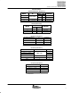
SN65HVD230 SN65HVD231 SN65HVD232 SLOS346G – MARCH 2001 – REVISED JUNE 2002 TYPICAL CHARACTERISTICS SUPPLY CURRENT (RMS) vs FREQUENCY LOGIC INPUT CURRENT (PIN D) vs INPUT VOLTAGE 33 0 –2 I I(L) – Logic Input Current – µ A I CC – Supply Current (RMS) – mA 32 31 30 29 28 27 26 25 –4 –6 –8 –10 –12 –14 0 250 500 –16 750 1000 1250 1500 1750 2000 f – Frequency – kbps Figure 10 3.1 3.6 160 I OL – Driver Low-Level Output Current – mA I I – Bus Input Current – µ A 1.1 1.6 2.1 2.
SN65HVD230 SN65HVD231 SN65HVD232 SLOS346G – MARCH 2001 – REVISED JUNE 2002 TYPICAL CHARACTERISTICS DRIVER HIGH-LEVEL OUTPUT CURRENT vs HIGH-LEVEL OUTPUT VOLTAGE DOMINANT VOLTAGE (VOD) vs FREE-AIR TEMPERATURE 3 VCC = 3.6 V 100 2.5 VOD– Dominant Voltage – V I OH – Driver High-Level Output Current – mA 120 80 60 40 20 0 VCC = 3.3 V VCC = 3 V 2 1.5 1 0.5 0 0.5 1 1.5 2 2.5 3 0 3.
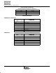
SN65HVD230 SN65HVD231 SN65HVD232 SLOS346G – MARCH 2001 – REVISED JUNE 2002 DRIVER LOW-TO-HIGH PROPAGATION DELAY TIME vs FREE-AIR TEMPERATURE 55 RS = 0 VCC = 3 V 50 45 40 VCC = 3.3 V 35 VCC = 3.6 V 30 25 20 15 10 –55 –40 0 25 70 85 125 t PHL– Driver High-to-Low Propagation Delay Time – ns t PLH – Driver Low-to-High Propagation Delay Time – ns TYPICAL CHARACTERISTICS DRIVER HIGH-TO-LOW PROPAGATION DELAY TIME vs FREE-AIR TEMPERATURE 90 RS = 0 VCC = 3.6 V 85 80 75 VCC = 3.
SN65HVD230 SN65HVD231 SN65HVD232 SLOS346G – MARCH 2001 – REVISED JUNE 2002 DRIVER LOW-TO-HIGH PROPAGATION DELAY TIME vs FREE-AIR TEMPERATURE 800 RS = 100 kΩ 700 VCC = 3 V 600 VCC = 3.3 V 500 VCC = 3.6 V 400 300 200 100 0 –55 –40 0 25 70 85 125 DRIVER HIGH-TO-LOW PROPAGATION DELAY TIME vs FREE-AIR TEMPERATURE t PHL– Driver High-to-Low Propagation Delay Time – ns t PLH – Driver Low-to-High Propagation Delay Time – ns TYPICAL CHARACTERISTICS 1000 RS = 100 kΩ VCC = 3.6 V 950 VCC = 3.
SN65HVD230 SN65HVD231 SN65HVD232 SLOS346G – MARCH 2001 – REVISED JUNE 2002 TYPICAL CHARACTERISTICS REFERENCE VOLTAGE vs REFERENCE CURRENT 3 V ref – Reference Voltage – V 2.5 2 VCC = 3.6 V 1.5 VCC = 3 V 1 0.5 0 –50 –5 5 50 Iref – Reference Current – µA Figure 26 APPLICATION INFORMATION This application provides information concerning the implementation of the physical medium attachment layer in a CAN network according to the ISO 11898 standard.
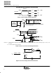
SN65HVD230 SN65HVD231 SN65HVD232 SLOS346G – MARCH 2001 – REVISED JUNE 2002 APPLICATION INFORMATION ISO 11898 Specification Implementation Application Specific Layer TMS320Lx2403/6/7 3.3-V DSP Logic Link Control Data-Link Layer Embedded Medium Access Control CAN Controller Physical Signaling Physical Layer Physical Medium Attachment SN65HVD230 Medium Dependent Interface CAN Bus-Line Figure 27.
SN65HVD230 SN65HVD231 SN65HVD232 SLOS346G – MARCH 2001 – REVISED JUNE 2002 APPLICATION INFORMATION Electronic Control Unit (ECU) TMS320Lx2403/6/7 CAN-Controller CANTX/IOPC6 CANRX/IOPC7 D R SN65HVD230 CANH CANL CAN Bus Line Figure 28. Details of a Typical CAN Node ECU 1 ECU 2 ECU n CANH 120 Ω CAN Bus Line 120 Ω CANL Figure 29. Typical CAN Network The SN65HVD230/231/232 3.3-V CAN transceivers provide the interface between the 3.
SN65HVD230 SN65HVD231 SN65HVD232 SLOS346G – MARCH 2001 – REVISED JUNE 2002 APPLICATION INFORMATION features of the SN65HVD230, SN65HVD231, and SN65HVD232 (continued) The bus pins are also maintained in a high-impedance state during low VCC conditions to ensure glitch-free power-up and power-down bus protection for hot-plugging applications. This high-impedance condition also means that an unpowered node does not disturb the bus. Transceivers without this feature usually have a very low output impedance.
SN65HVD230 SN65HVD231 SN65HVD232 SLOS346G – MARCH 2001 – REVISED JUNE 2002 APPLICATION INFORMATION high-speed (continued) 1 Mbps Driver Output NRZ Data 1 Figure 31. Typical High Speed SN65HVD230 Output Waveform Into a 60-Ω Load slope control Electromagnetic compatibility is essential in many applications using unshielded bus cable to reduce system cost.
SN65HVD230 SN65HVD231 SN65HVD232 SLOS346G – MARCH 2001 – REVISED JUNE 2002 APPLICATION INFORMATION DRIVER OUTPUT SIGNAL SLOPE vs SLOPE CONTROL RESISTANCE Driver Outout Signal Slop – V/ µ s 25 20 15 10 5 0 0 10 4.7 20 30 40 50 33 60 47 70 6.8 10 15 22 Slope Control Resistance – kΩ 80 68 90 100 Figure 33. HVD230 Driver Output Signal Slope vs Slope Control Resistance Value RS = 0 Ω RS = 10 kΩ RS = 100 kΩ Figure 34. Typical SN65HVD230 250-kbps Output Pulse Waveforms With Slope Control www.ti.
SN65HVD230 SN65HVD231 SN65HVD232 SLOS346G – MARCH 2001 – REVISED JUNE 2002 APPLICATION INFORMATION standby mode (listen only mode) of the HVD230 If a logic high (> 0.75 VCC) is applied to RS (pin 8) in Figures 30 and 32, the circuit of the SN65HVD230 enters a low-current, listen only standby mode, during which the driver is switched off and the receiver remains active. In this listen only state, the transceiver is completely passive to the bus.
SN65HVD230 SN65HVD231 SN65HVD232 SLOS346G – MARCH 2001 – REVISED JUNE 2002 APPLICATION INFORMATION ( ) Figure 35. 70.7-ns Loop Delay Through the HVD230 With RS = 0 www.ti.
SN65HVD230 SN65HVD231 SN65HVD232 SLOS346G – MARCH 2001 – REVISED JUNE 2002 APPLICATION INFORMATION interoperability with 5-V CAN systems It is essential that the 3.3-V HVD230 family performs seamlessly with 5-V transceivers because of the large number of 5-V devices installed. Figure 36 displays a test bus of a 3.3-V node with the HVD230, and three 5-V nodes: one for each of TI’s SN65LBC031 and UC5350 transceivers, and one using a competitor X250 transceiver.
SN65HVD230 SN65HVD231 SN65HVD232 SLOS346G – MARCH 2001 – REVISED JUNE 2002 APPLICATION INFORMATION Driver Input CAN Bus Receiver Output Figure 37. The HVD230’s Input, CAN Bus, and X250’s RXD Output Waveforms Figure 37 displays the HVD230’s input signal, the CAN bus, and the competitor X250’s receiver output waveforms. The input waveform from the Tektronix HFS-9003 Pattern Generator in Figure 36 to the HVD230 is a 250-kbps pulse for this test.
SN65HVD230 SN65HVD231 SN65HVD232 SLOS346G – MARCH 2001 – REVISED JUNE 2002 MECHANICAL DATA D (R-PDSO-G**) PLASTIC SMALL-OUTLINE PACKAGE 14 PINS SHOWN 0.050 (1,27) 0.020 (0,51) 0.014 (0,35) 14 0.010 (0,25) M 8 0.008 (0,20) NOM 0.244 (6,20) 0.228 (5,80) 0.157 (4,00) 0.150 (3,81) Gage Plane 0.010 (0,25) 1 7 0°–ā8° A 0.044 (1,12) 0.016 (0,40) Seating Plane 0.069 (1,75) MAX 0.010 (0,25) 0.004 (0,10) PINS ** 0.004 (0,10) 8 14 16 A MAX 0.197 (5,00) 0.344 (8,75) 0.394 (10,00) A MIN 0.
IMPORTANT NOTICE Texas Instruments Incorporated and its subsidiaries (TI) reserve the right to make corrections, modifications, enhancements, improvements, and other changes to its products and services at any time and to discontinue any product or service without notice. Customers should obtain the latest relevant information before placing orders and should verify that such information is current and complete.