
CAN Board - Datasheet
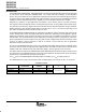
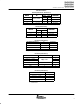
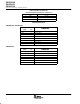
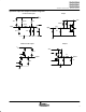
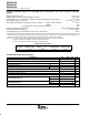
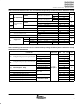
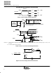
Table Of Contents
- FEATURES
- APPLICATIONS
- DESCRIPTION
- Function Tables
- Terminal Functions
- equivalent input and output schematic diagrams
- absolute maximum ratings over operating free-air temperature (see Note \ 1) (unless otherwise noted) †
- recommended operating conditions
- ELECTRICAL SPECIFICATIONS
- driver electrical characteristics over recommended operating conditions \ (unless otherwise noted)
- driver switching characteristics over recommended operating conditions(\ unless otherwise noted)
- receiver electrical characteristics over recommended operating condition\ s (unless otherwise noted)
- receiver switching characteristics over recommended operating conditions\ (unless otherwise noted)
- device switching characteristics over recommended operating conditions (\ unless otherwise noted)
- device control-pin characteristics over recommended operating conditions\ (unless otherwise noted)
- PARAMETER MEASUREMENT INFORMATION
- TYPICAL CHARACTERISTICS
- APPLICATION INFORMATION
- MECHANICAL DATA
- IMPORTANT NOTICE

SN65HVD230
SN65HVD231
SN65HVD232
SLOS346G – MARCH 2001 – REVISED JUNE 2002
10
www.ti.com
PARAMETER MEASUREMENT INFORMATION
≈ 2.3 V
Dominant
Recessive
CANL
V
OL
≈ 3 V
V
OH
≈ 1 V
V
OH
CANH
CANH
CANL
Figure 3. Driver Output Voltage Definitions
V
O
R
L
= 60 Ω
50 Ω
Signal
Generator
(see Note A)
C
L
= 50 pF
(see Note B)
90%
Output
0.9 V
10%
t
f
V
OD(R)
V
OD(D)
t
r
Input
0 V
3 V
t
PHL
1.5 V
t
PLH
R
S
= 0 Ω to 100 kΩ for SN65HVD230 and SN65HVD231
N/A for SN65HVD232
0.5 V
NOTES: A. The input pulse is supplied by a generator having the following characteristics: PRR ≤ 500 kHz, 50% duty cycle, t
r
≤ 6 ns, t
f
≤ 6 ns,
Z
o
= 50 Ω.
B. C
L
includes probe and jig capacitance.
Figure 4. Driver Test Circuit and Voltage Waveforms
V
IC
+
V
CANH
) V
CANL
2
V
ID
V
O
V
CANL
V
CANH
I
O
Figure 5. Receiver Voltage and Current Definitions