
CAN Board - Datasheet
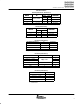
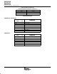
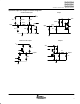
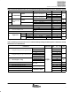
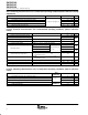
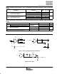
Table Of Contents
- FEATURES
- APPLICATIONS
- DESCRIPTION
- Function Tables
- Terminal Functions
- equivalent input and output schematic diagrams
- absolute maximum ratings over operating free-air temperature (see Note \ 1) (unless otherwise noted) †
- recommended operating conditions
- ELECTRICAL SPECIFICATIONS
- driver electrical characteristics over recommended operating conditions \ (unless otherwise noted)
- driver switching characteristics over recommended operating conditions(\ unless otherwise noted)
- receiver electrical characteristics over recommended operating condition\ s (unless otherwise noted)
- receiver switching characteristics over recommended operating conditions\ (unless otherwise noted)
- device switching characteristics over recommended operating conditions (\ unless otherwise noted)
- device control-pin characteristics over recommended operating conditions\ (unless otherwise noted)
- PARAMETER MEASUREMENT INFORMATION
- TYPICAL CHARACTERISTICS
- APPLICATION INFORMATION
- MECHANICAL DATA
- IMPORTANT NOTICE

SN65HVD230
SN65HVD231
SN65HVD232
SLOS346G – MARCH 2001 – REVISED JUNE 2002
6
www.ti.com
absolute maximum ratings over operating free-air temperature (see Note 1) (unless otherwise
noted)
†
Supply voltage range, V
CC
–0.3 V to 6 V. . . . . . . . . . . . . . . . . . . . . . . . . . . . . . . . . . . . . . . . . . . . . . . . . . . . . . . . . . . . . . .
Voltage range at any bus terminal (CANH or CANL) –4 V to 16 V. . . . . . . . . . . . . . . . . . . . . . . . . . . . . . . . . . . . . . . . . .
Voltage input range, transient pulse, CANH and CANL, through 100 Ω (see Figure 7) –25 V to 25 V. . . . . . . . . . . .
Input voltage range, V
I
(D or R) –0.5 V to V
CC
+ 0.5 V. . . . . . . . . . . . . . . . . . . . . . . . . . . . . . . . . . . . . . . . . . . . . . . . . . .
Electrostatic discharge: Human body model (see Note 2) CANH, CANL and GND 16 kV. . . . . . . . . . . . . . . . . .
All Pins 4 kV. . . . . . . . . . . . . . . . . . . . . . . . . . . . . . . . . .
Charged-device model (see Note 3) All pins 1 kV. . . . . . . . . . . . . . . . . . . . . . . . . . . . . . . . . .
Continuous total power dissipation See Dissipation Rating table. . . . . . . . . . . . . . . . . . . . . . . . . . . . . . . . . . . . . . . . . . .
Storage temperature range, T
stg
–65°C to 150°C. . . . . . . . . . . . . . . . . . . . . . . . . . . . . . . . . . . . . . . . . . . . . . . . . . . . . . . .
Lead temperature 1,6 mm (1/16 inch) from case for 10 seconds 260°C. . . . . . . . . . . . . . . . . . . . . . . . . . . . . . . . . . . . .
†
Stresses beyond those listed under “absolute maximum ratings” may cause permanent damage to the device. These are stress ratings only, and
functional operation of the device at these or any other conditions beyond those indicated under “recommended operating conditions” is not
implied. Exposure to absolute-maximum-rated conditions for extended periods may affect device reliability.
NOTES: 1. All voltage values, except differential I/O bus voltages, are with respect to network ground terminal.
2. Tested in accordance with JEDEC Standard 22, Test Method A114-A.
3. Tested in accordance with JEDEC Standard 22, Test Method C101.
DISSIPATION RATING TABLE
PACKAGE
T
A
≤ 25°C
POWER RATING
DERATING FACTOR
‡
ABOVE T
A
= 25°C
T
A
= 70°C
POWER RATING
T
A
= 85°C
POWER RATING
D 725 mW 5.8 mW/°C 464 mW 377 mW
‡
This is the inverse of the junction-to-ambient thermal resistance when board-mounted and with no air flow.
recommended operating conditions
PARAMETER MIN NOM MAX UNIT
Supply voltage, V
CC
3 3.6 V
Voltage at any bus terminal (common mode) V
IC
–2
§
7 V
Voltage at any bus terminal (separately) V
I
–2.5 7.5 V
High-level input voltage, V
IH
D, R 2 V
Low-level input voltage, V
IL
D, R 0.8 V
Differential input voltage, V
ID
(see Figure 5) –6 6 V
Input voltage, V
(Rs)
0 V
CC
V
Input voltage for standby or sleep, V
(Rs)
0.75 V
CC
V
CC
V
Wave-shaping resistance, Rs 0 100 kΩ
High level output current I
Driver –40
mA
High-level output current, I
OH
Receiver –8
mA
Low level output current I
Driver 48
mA
Low-level output current, I
OL
Receiver 8
mA
Operating free-air temperature, T
A
–40 85 °C
§
The algebraic convention, in which the least positive (most negative) limit is designated as minimum is used in this data sheet.